基板クイック試作
カスタム基板試作サービス
基板クイック試作
カスタム基板試作サービス
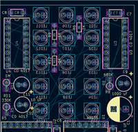
Reason of failed review:
The lengends in solder mask layer is required to be min 1.2mm at height,and 0.2mm at width.And the min spacing between lengends should be 0.2mm at least.
Suggestion:
It’s advised to measure the size and spacing when you upload the gerber file for review,and you can ask your sales rep to help you confirm if you have issue in checking this information.