基板クイック試作

カスタム基板試作サービス

PCBアセンブリFAQ

最も費用対効果が高く、高品質のPCB製造業者およびPCBAサービスプロバイダーの1つとして、私たちは研究業務に100人以上の新しいエンジニアが私たちのサービスを利用しています。 ビジネス:私達は私達の新しい顧客が私達の製品やサービスについて知るためにこれらの質問をまとめます。
More details: Check our SMT FAQs page.
PCB Assembly Ordering
SMT Engineering Questions
Components question
Assembly files problems

Q:1.PCBWay.comはだれですか。

PCBWayは、PCBのプロトタイピング、少量生産、およびPCB組み立てサービスを1つの屋根の下で行う、中国の深センに拠点を置くメーカーです。PCBWay –基板クイック試作!

Q:2.あなたはPCBWayによって作られていないボードを組み立てることを受け入れますか?

現在、他社のPCBを使用して施設内で組み立てることはしていませんが、お客様の時間と費用を節約するために、PCB製造、部品調達、およびPCB組み立てを連続的かつ円滑に行っています。

Q:3.私のPCBA注文に対してどのようなファイルや文書を要求しますか?

私達にあなたのPCBの発注のためのGerberファイル、CentroidデータおよびBOMがある私達と既にあなたのPCBの発注をしたように、実際にあなたはあなたのPCB Gerberファイルがシルクスクリーン、銅トラックおよびはんだののりの層を含んでいれば PCB Gerberファイルに上記の3つの層のいずれかが欠けている場合は、これがPCBAの最低限の要求であるため、それらを再送信してください。 あいまいで部品の配置が間違っていることもありますが、ほとんどのアセンブラーでは必要ありません。

Q:4.Centroidとは何ですか?

Centroidは、アセンブリマシンをすばやくプログラミングするために使用されるアセンブリ用の特殊ファイルで、別名Insertion、Pick-N-Place、またはXY Dataとも呼ばれます。 Centroidファイルには、すべての表面実装部品の位置と方向が記述されており、参照指定子、XとYの位置、回転とボードの側面(上または下)のみが含まれています。 表面実装部品はセントロイドに記載されています。

Q:5.受託注文またはキット注文の部品の出荷およびマーキングはどのように依頼しますか?

個々のパッケージや箱にBOM、製造元の部品番号、または顧客の部品番号、数量の対応する行番号をマークできることを願っています。

Q:6.受託/キッティングされたPCBAの部品の過給に対するあなたの要求は何ですか?

Unused and excessive parts supplied by you or purchased by us will not be returned by default. If you want the parts to be sent back to you with the assembled boards, please contact your service representitive or make a note on your related order, and let us know which parts to send.

リールに供給されていないSMT部品は、1本の連続したテープの上になければなりません。

同じSMT部品を異なるボードに組み立てる必要がある場合は、それらをストリップにカットしないでください。テープの連続ストリップまたはリールに保管してください。

抵抗器、コンデンサ、ダイオード(0603、0805、1206、2225、SOT、SOD、MELF - パッケージ)は最小50個必要で、必要な数量を30個超える必要があります(例:数量40個の組み立て - 必要になります)。 70個 - これは私達の最低50個と組立量の30個以上を満たしています。

抵抗器、コンデンサ、ダイオード(0201、0402、miniMelf、ミニチュアパッケージ)は、最低100個が必要量を50個超えなければなりません(例:組み立て数量80個 - これは最低限130個必要です)。 100個プラス50個以上の組み立て数量)

IC, BGA, QFP,コネクタなどの高価な部品について,少量の余分な(部品の総数に基づく1-5件)を必要とし,それは顺调に组み立てられ,时间通りにあなたの组み立て板を出荷することを确保する。もし質問や質問があれば、私たちにもっと情報を送ったり連絡して回答を獲得してください。

Q:7.私のアセンブリ用にいくつかの部品を調達できますか?

あなたはいくつかの部品を供給するかもしれません、そして、我々はあなたに代わって部品の残りを調達します。 代用が必要です、我々は再びあなたの最終的な承認を求めます。

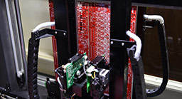
Q:8. BGAを組み立てますか?これに関する特別な要件はありますか?

はい、X線検査で0.25mmピッチのBGAを処理する能力があります。BGAの場合、2つの設計があります。1つは、穴がパッド上にあること、もう1つは、穴がパッドの隣にあり、パターンの近くにあることです。溶接の品質を確保するために、BGAのパッド近くのビアにレジストカバーする必要があります。また、パッド上のビアについては、良好な溶接の品質を確保するためにビアに樹脂を充填する必要があります。

Q:9.余分な未使用の部品はどのように取り扱っていますか?

余分な部品が存在するのは、委託/キッド注文の場合、超過分の何パーセントかを請求するか、これらのターンキー注文の場合と同じ目的で購入するためです。 積まれた板、またはあなたの次の順序のための私達の棚にそれらを保ちなさい。

Q:10. PCBAサービスの合計金額をどのように見積もりますか?

当社のオンラインインスタント見積システムでは、工具、レーザーカットスチールステンシル、および人件費を含むPCBAのコストの大まかなアイデアが示されていますターンキーまたは部分的なターンキーPCBAの場合は、部品のコストが追加されます。

Q:11.ターンタイムはいつ始まりますか?

PCBAサービスの納期を決定する方法は複雑であるため、すべての部品とPCBの準備が整い、すべてのPCBファイル(Gerberファイル/その他のPCBファイルなど)が完成した直後に納期が開始されることが当社の方針です。 Centroid(ピックアンドプレースPNPファイル、またはXYデータまたは他の形式のファイル)、BOM、およびその他すべての必要なデータまたは文書/画像/写真が完成しています。

Q:12.アセンブリはRoHSに準拠していますか?

Yes. But we also offer leaded PCBA services.

Q:13.ボードをパネライズする必要があるのはなぜですか?

PCBの寸法が50mmx100mmよりも小さい場合、またはPCBが長方形以外の任意の形状(円形、または奇数形状)の場合は、パネル化が必要です。また、アセンブリ用にアレイでパネル化する必要があります。 だから私たちはあなたのボードを製作します。私たちはパネル化ファイル(はんだペーストデータ)を持っているでしょう、私たちはパネル化されたPCBと一致するステンシルを作成するためにPCBA部門にデータを転送します。

Q:14.分離レール(分離タブ)を設計する必要があるのはなぜですか?

ボードの端と銅の部分との間隔が3.5mm(138mil)未満の場合、または何らかの理由でパネルをパネル化する必要がある場合は、2本の長い平行端にブレークアウェイレール(タブ)を追加してください。 ボードが機械によって組み立てられることを確実にするためのボードこれはボードがSMT機械によって処理されることを可能にします。

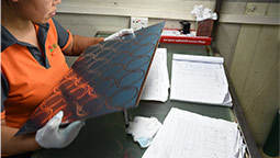
Q:15.組み立てたボードを受け取った後に欠陥や問題が見つかった場合はどうすればいいですか?

PCBAは多くの詳細を含む複雑な作品であるため、時々欠陥や問題が発生する可能性がありますあなたが欠陥や問題を見つけた場合は、すぐに私たちに知らせてください。 私達はあなたのボードを修理するか、手直しするか、またはリメイクします欠陥のあるボードを必要とするならば、私たちはあなたに私達にそれらを送り返すように頼むかもしれません。

Q:16.あなたのPCBアセンブリ標準は何ですか。

IPC-A-610 Class 2.

Q:17.ターンキー注文でのあなたのターン時間は?

すべての部品をターンキー注文のために調達する必要があるので、ターンタイムの主な要素は、すべての部品をどれだけ早く入手できるかによって異なります。 部品を手に入れたらすぐに組み立てができるように、ステンシルを作り始めます。

お問い合わせ!

私達のカスタマーサービス
あなたのPCBの準備ができて

+86-571-85317532

quotesI am impressed with the quality of the boards, the delivery time and responce to all my questions. Best price excellent service and speedy delivery. When I need another board I will certainly use this supplier. "

-Bill Robinson Company

quotesспасибо за платы! платы очень хорошего качества. надежный продавец. оперативно отвечал на вопросы. заказ выполнили и отправили очень быстро.Заказываю платы не в первый раз - как всегда только лучшие впечатления. 5+++. 4 числа отправил файлы 26-го забрал на почте в Москве."

-FVL. SKU Company
Front-end data preparation

01.PPE - Pre Production Engineering

Customer supplied data (gerber) is used to produce the manufacturing data for the specific PCB (artworks for imaging processes and drill data for drilling programs). Engineers compare demands/specifications against capabilities to ensure compliance and also determine the process steps and associated checks. No changes are allowed without PCBWay Group permission.

Preparing

02.Preparing the phototools

Artwork Master is PCB production in the key steps, which directly affect the quality of the final product quality,An accurately scaled configuration of electronic data used to produce the artwork master or production master. Artwork Master – The photographic image of the PCB pattern on film used to produce the circuit board, usually on a 1:1 scale.In general, there are three types of Artwork Master:(1) Conductive Pattern  (2) solder mask (3) Silkscreen

print icon

03.Print inner layers

Stage 1 is to transfer the image using an artwork film to the board surface, using photosensitive dry-film and UV light, which will polymerise the dry film exposed by the artwork.
This step of the process is performed in a clean room.
Imaging – The process of transferring electronic data to the photo-plotter, which in turn uses light to transfer a negative image circuitry pattern onto the panel or film.

etch icon

04.Etch inner layers

Stage 2 is to remove the unwanted copper from the panel using etching. Once this copper has been removed, the remaining dry film is then removed leaving behind the copper circuitry that matches the design.
Etching – The chemical, or chemical and electrolytic, removal of unwanted portions of conductive or resistive material.

aoi icon

05.Inner layer Automatic Optical Inspection(AOI)

Inspection of the circuitry against digital “images” to verify that the circuitry matches the design and that it is free from defects. Achieved through scanning of the board and then trained inspectors will verify any anomalies that the scanning process has highlighted. PCBWay Group allows no repair of open circuits.

Lamination icon

06.Lay-up and bond (Lamination)

The inner layers have an oxide layer applied and then “stacked” together with pre-preg providing insulation between layers and copper foil is added to the top and bottom of the stack. The lamination process consists of placing the internal layers under extreme temperature (375 degrees Fahrenheit) and pressure (275 to 400 psi) while laminating with a photosensitive dry resist. The PCB is allowed to cure at a high temperature, the pressure is slowly released and then the material is slowly cooled.

drilling icon

07.Drilling the PCB

We now have to drill the holes that will subsequently create electrical connections within the multilayer PCB. This is a mechanical drilling process that must be optimised so that we can achieve registration to all of the the inner layer connections. The panels can be stacked at this process. The drilling can also be done by a laser drill

copper icon

08.Electroless copper deposition

The first step in the plating process is the chemical deposition of a very thin layer of copper on the hole walls.
PTH provides a very thin deposit of copper that covers the hole wall and the complete panel. A complex chemical process that must be strictly controlled to allow a reliable deposit of copper to be plated even onto the non-metallic hole wall. Whilst not a sufficient amount of copper on its own, we now have electrical continuity between layers and through the holes.Panel plating follows on from PTH to provide a thicker deposit of copper on top of the PTH deposit – typically 5 to 8 um. The combination is used to optimise the amount of copper that is to be plated and etched in order to achieve the track and gap demands.

image icon

09.Image the outer layers

Similar to the inner layer process (image transfer using photosensitive dry film, exposure to UV light and etching), but with one main difference – we will remove the dry film where we want to keep the copper/define circuitry – so we can plate additional copper later in the process.
This step of the process is performed in a clean room.

Plating icon

10.Plating

Second electrolytic plating stage, where the additional plating is deposited in areas without dry film (circuitry). Once the copper has been plated, tin is applied to protect the plated copper.

etch icon

11.Etch outer layer

This is normally a three step process. The first step is to remove the blue dry film. The second step is to etch away the exposed/unwanted copper whilst the tin deposit acts an etch resist protecting the copper we need. The third and final step is to chemically remove the tin deposit leaving the circuitry.

AOI

12.Outer layer AOI

Just like with inner layer AOI the imaged and etched panel is scanned to make sure that the circuitry meets design and that it is free from defects. Again no repair of open circuits are allowed under PCBWay demands.

Soldermask

13.Soldermask

Soldermask ink is applied over the whole PCB surface. Using artworks and UV light we expose certain areas to the UV and those areas not exposed are removed during the chemical development process – typically the areas which are to be used as solderable surfaces. The remaining soldermask is then fully cured making it a resilient finish.
This step of the process is performed in a clean room.

Surface finish

14.Surface finish

Various finishes are then applied to the exposed copper areas. This is to enable protection of the surface and good solderability. The various finishes can include Electroless Nickel Immersion Gold, HASL, Immersion Silver etc. Thicknesses and solderability tests are always carried out.

Profile

15.Profile

This is the process of cutting the manufac-turing panels into specific sizes and shapes based upon the customer design as defined within the gerber data. There are 3 main options available when providing the array or selling panel – scoring, routing or punching. All dimensions are measured against the customer supplied drawing to ensure the panel is dimensionally correct.

Electrical test

16.Electrical test

Used for checking the integrity of the tracks and the through hole interconnections – checking to ensure there are no open circuits or no short circuits on the finished board. There are two test methods, flying probe for smaller volumes and fixture based for volumes.We electrically test every multilayer PCB against the original board data. Using a flying probe tester we check each net to ensure that it is complete (no open circuits) and does not short to any other net.

inspection

17.Final inspection

In the last step of the process a team of sharp-eyed inspectors give each PCB a final careful check-over.Visual checking the PCB against acceptance criteria and using PCBWay “approved” inspectors. Using manual visual inspection and AVI – compares PCB to gerber and has a faster checking speed that human eyes, but still requires human verification. All orders are also subjected to a full inspection including dimensional, solderability, etc.

Packaging

18.Packaging

Boards are wrapped using materials that comply with the PCBWay Packaging demands (ESD etcetera) and then boxed prior to be being shipped using the requested mode of transport.