基板クイック試作
カスタム基板試作サービス
基板クイック試作
カスタム基板試作サービス
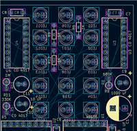
Reason of failed review:
The spacing from unplated slot to copper trace should be ≧ 0.2mm. See pointed area, this unplated slot will cut the copper trace off. When you route the slots, the nearby copper traces will be definitely damaged.
Suggestion:
1.Customer accept to cut partial pad to guarantee the minimum 0.2mm spacing from unplated slot to copper trace?
2. Modify design to move the copper traces or the slot a little bit to meet the requirement of 0.2mm spacing.