基板クイック試作
カスタム基板試作サービス
基板クイック試作
カスタム基板試作サービス
もともと、すべてのPCBははんだごてだけを使って手作業で組み立てられていました。 技術が進歩するにつれて、構成要素は手で組み立てることがより小さくそしてより困難になり、そして単一のボード上に収まることができる構成要素の量は増加する。 そのため、自動組立の必要性が生まれました。

以下は自動実装に必要な要素です:
Gerbers in 274-X (embedded apertures) including fabrication drawing.
Part centroid text file with Reference Designators, external placement layer, and X & Y location and rotation in ASCII format.
Numerical control (NC) drill files
Solder paste file (one of the Gerber files) for all sides mounted
Glue dot file
可能であれば、データベースを設計し、データベース形式(プログラム名)を指定してください。
部品リストまたはBOM(部品表)
必要な部品またはハードウェア
Gerberファイルはパッドの位置を定義し、アセンブリハウスがピン1の位置を決定し、ボードの外観を把握するのに役立ちますデータベースはピン1の位置を決定するのにも使用できます。 どのように、そしてなぜ集会所がステンシルを作るのかを学び、それを複製してそれぞれから一貫性を保つのは良いことです。 はんだペーストファイルは、はんだ付けされる部分を除いてボード全体をマスクするために使用され、露出したパッドにはんだペーストが塗布され、ステンシルが除去されます。 また、部品が基板にはんだ付けされるときに、部品を固定しているはんだペーストと接着剤の点で基板に固定されます。
部品配置の場合、部品配置/centroidファイルで部品の部品がどこにあるのかを知る必要がありますレイヤIDは部品が配置されている側を示し、回転は部品の向きを表示します。
設計者のソフトウェアが矛盾を考慮できない場合を除き、元のコンポーネントの回転の一貫性が重要です。
NCドリルファイルを使用して、取り付け穴の位置を特定し、スルーホール部品の穴サイズを提供しますこれにより、組み立て工場でも部品リードの適切なクリアランスを決定できます。
部品表または部品リストを使用して、centroidファイルの指示子およびマウントする必要があるコンポーネントを参照します。 部品がSM部品なのかDIP部品なのかについても、BOMは情報を提供する必要があります。
自動組み立てに関するその他の考慮事項は、ボードサイズ、パネルサイズ、およびブレークアウェイです。 ボードは一般的に多くのボードを含むことができるパネルに組み立てられます。 パネルは、ボードがエッチングされた元の素材です。パネルは、すべてのボードがそのままの状態で組み立て工場に渡されます。
説明
Breakawaysは、組み立て中にボードを保持するボード周囲の接続ですが、ボードを取り外すときには簡単に壊れる可能性があります。
PCBWayワンストップ基板と部品実装ソリューション,
The DFM check looks at all the design specifications of a PCB. Specifically, this check looks for any missing, redundant or potentially problematic features. Any of these issues may severely and negatively influence the functionality of the final project. For example, one common PCB design flaw is leaving too little spacing between PCB components. This can result in shorts and other malfunctions.
By identifying potential problems before manufacturing begins, DFM checks can cut manufacturing costs and eliminate unforeseen expenses. This is because these checks cut down on the number of scrapped boards. As part of our commitment to quality at a low cost.

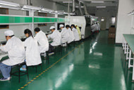
PCBWay Verifying all incoming materials and handling quality problems before subsequent SMT assembly begins. Our IQC position will check following issues of incoming materials if they comply with our strict requirements.
• BOMリストに基づく型番と数量をリストアップする
• 特にICまたはその他の複雑なコンポーネントの形状(変形、破損したピン、酸化など)
• テストスタンドやマルチメーターなどのツールを使用した材料のサンプルテスト。
• 上記の欠陥または不一致が発生した場合、当社はすべての材料をサプライヤーまたは顧客に返却します。
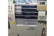
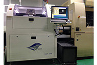
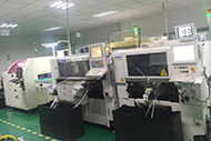
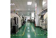
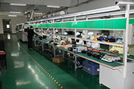
Having received the PCB panels and components the next step is to setup the various machines used with the manufacturing process. Machines such as the placement machine and AOI (Automated Optical Inspection) will require a program to be created which is best generated from CAD data but quite often this isn't available. Gerber data is almost always available as this is the data required for the bare PCB to be manufactured.
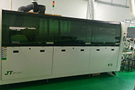
製造プロセスでセットアップする最初のマシンは、PCB上の適切なパッドにステンシルとスキージを使用してはんだペーストを塗布するように設計されたはんだペーストプリンタです。

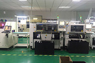
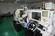
Once the printed PCB has been confirmed to have the correct amount of solder paste applied it moves into the next part of the manufacturing process which is component placement. Each component is picked from its packaging using either a vacuum or gripper nozzle, checked by the vision system and placed in the programed location at high speed.
There is a large variety of machines available for this process and it depends greatly on the business to what type of machine is selected. For example if the business is focused around large build quantities then the placement rate will be important however if the focus is small batch/high mix then flexibility will be more important.

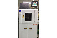
コンポーネントの配置プロセスに続いて、リフローはんだ付けの前に間違いがなく、すべての部品が正しく配置されていることを確認することが重要です。 これを行う最良の方法は、AOIマシンを使用して、コンポーネントの存在、タイプ/値、極性などのチェックを行うことです。

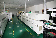
Once the components are placed on the boards, each piece is sent through our reflow machines. This means the solder paste needs to solidify, adhering components to the board. PCB assembly accomplishes this through a process called "reflow".
This would appear to be one of the less complicated parts of the assembly processes but the correct reflow profile is key to ensure acceptable solder joints without damaging the parts or assembly due to excessive heat.
When using lead-free solder a carefully profiled assembly is even more important as the required reflow temperature can often be very close to many components maximum rated temperature.

The last part of the surface mount assembly process is to again check that no mistakes have been made by using an AOI machine to check solder joint quality.
Often, movement during the reflow process will result in poor connection quality or a complete lack of a connection. Shorts are also a common side effect of this movement, as misplaced components can sometimes connect portions of the circuit that should not connect.
Checking for these errors and misalignments can involve one of several different inspection methods. The most common of these inspection methods include the following:

Some completed Printed Circuit Board Assemblies have a conformal coating. It's usually depends on the customer's product requirements.
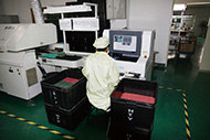
After the soldering and conformal coating step of the PCB assembly process is finished, a final inspection will test the PCB for its functionality by our Quality Assurance team. This inspection is known as a "functional test". The test software and tools are usually provided by the customer, PCBWay can also make fixtures according to customer requirements. The test puts the PCB through its paces, simulating the normal circumstances in which the PCB will operate. Power and simulated signals run through the PCB in this test while testers monitor the PCB's electrical characteristics.
Suffice it to say, the manufacturing process can be a filthy one. Soldering paste leaves behind some amount of flux, while human handling can transfer oils and dirt from fingers and clothing to the surface of the board. Once all is said and done, the results can look a little dingy, which is both an aesthetic and a practical issue.

組み立てられたボードはすべてきちんと包装され(帯電防止パッケージで要求できます)、出荷されたDHL、FedEx、UPS、EMSなどです。 未使用のコンポーネントは、顧客の指示に従って返却されます。 さらに、パッケージが出荷されると、顧客に電子メールで通知されます。

お問い合わせ!
私達のカスタマーサービス+86-571-85317532
Great place to get all of my PCB's printed. Did a great job and held my hand through any question I had.
Long
Great place to get all of my PCB's printed. Did a great job and held my hand through any question I had.
Long

Customer supplied data (gerber) is used to produce the manufacturing data for the specific PCB (artworks for imaging processes and drill data for drilling programs). Engineers compare demands/specifications against capabilities to ensure compliance and also determine the process steps and associated checks. No changes are allowed without PCBWay Group permission.


Artwork Master is PCB production in the key steps, which directly affect the quality of the final product quality,An accurately scaled configuration of electronic data used to produce the artwork master or production master. Artwork Master – The photographic image of the PCB pattern on film used to produce the circuit board, usually on a 1:1 scale.In general, there are three types of Artwork Master:(1) Conductive Pattern (2) solder mask (3) Silkscreen


Stage 1 is to transfer the image using an artwork film to the board surface, using photosensitive dry-film and UV light, which will polymerise the dry film exposed by the artwork.
This step of the process is performed in a clean room.
Imaging – The process of transferring electronic data to the photo-plotter, which in turn uses light to transfer a negative image circuitry pattern onto the panel or film.


Stage 2 is to remove the unwanted copper from the panel using etching. Once this copper has been removed, the remaining dry film is then removed leaving behind the copper circuitry that matches the design.
Etching – The chemical, or chemical and electrolytic, removal of unwanted portions of conductive or resistive material.


Inspection of the circuitry against digital “images” to verify that the circuitry matches the design and that it is free from defects. Achieved through scanning of the board and then trained inspectors will verify any anomalies that the scanning process has highlighted. PCBWay Group allows no repair of open circuits.


The inner layers have an oxide layer applied and then “stacked” together with pre-preg providing insulation between layers and copper foil is added to the top and bottom of the stack. The lamination process consists of placing the internal layers under extreme temperature (375 degrees Fahrenheit) and pressure (275 to 400 psi) while laminating with a photosensitive dry resist. The PCB is allowed to cure at a high temperature, the pressure is slowly released and then the material is slowly cooled.


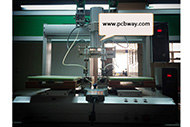
We now have to drill the holes that will subsequently create electrical connections within the multilayer PCB. This is a mechanical drilling process that must be optimised so that we can achieve registration to all of the the inner layer connections. The panels can be stacked at this process. The drilling can also be done by a laser drill


The first step in the plating process is the chemical deposition of a very thin layer of copper on the hole walls.
PTH provides a very thin deposit of copper that covers the hole wall and the complete panel. A complex chemical process that must be strictly controlled to allow a reliable deposit of copper to be plated even onto the non-metallic hole wall. Whilst not a sufficient amount of copper on its own, we now have electrical continuity between layers and through the holes.Panel plating follows on from PTH to provide a thicker deposit of copper on top of the PTH deposit – typically 5 to 8 um. The combination is used to optimise the amount of copper that is to be plated and etched in order to achieve the track and gap demands.


Similar to the inner layer process (image transfer using photosensitive dry film, exposure to UV light and etching), but with one main difference – we will remove the dry film where we want to keep the copper/define circuitry – so we can plate additional copper later in the process.
This step of the process is performed in a clean room.


Second electrolytic plating stage, where the additional plating is deposited in areas without dry film (circuitry). Once the copper has been plated, tin is applied to protect the plated copper.


This is normally a three step process. The first step is to remove the blue dry film. The second step is to etch away the exposed/unwanted copper whilst the tin deposit acts an etch resist protecting the copper we need. The third and final step is to chemically remove the tin deposit leaving the circuitry.


Just like with inner layer AOI the imaged and etched panel is scanned to make sure that the circuitry meets design and that it is free from defects. Again no repair of open circuits are allowed under PCBWay demands.


Soldermask ink is applied over the whole PCB surface. Using artworks and UV light we expose certain areas to the UV and those areas not exposed are removed during the chemical development process – typically the areas which are to be used as solderable surfaces. The remaining soldermask is then fully cured making it a resilient finish.
This step of the process is performed in a clean room.


Various finishes are then applied to the exposed copper areas. This is to enable protection of the surface and good solderability. The various finishes can include Electroless Nickel Immersion Gold, HASL, Immersion Silver etc. Thicknesses and solderability tests are always carried out.


This is the process of cutting the manufac-turing panels into specific sizes and shapes based upon the customer design as defined within the gerber data. There are 3 main options available when providing the array or selling panel – scoring, routing or punching. All dimensions are measured against the customer supplied drawing to ensure the panel is dimensionally correct.


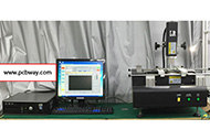
Used for checking the integrity of the tracks and the through hole interconnections – checking to ensure there are no open circuits or no short circuits on the finished board. There are two test methods, flying probe for smaller volumes and fixture based for volumes.We electrically test every multilayer PCB against the original board data. Using a flying probe tester we check each net to ensure that it is complete (no open circuits) and does not short to any other net.


In the last step of the process a team of sharp-eyed inspectors give each PCB a final careful check-over.Visual checking the PCB against acceptance criteria and using PCBWay “approved” inspectors. Using manual visual inspection and AVI – compares PCB to gerber and has a faster checking speed that human eyes, but still requires human verification. All orders are also subjected to a full inspection including dimensional, solderability, etc.


Boards are wrapped using materials that comply with the PCBWay Packaging demands (ESD etcetera) and then boxed prior to be being shipped using the requested mode of transport.