基板クイック試作
カスタム基板試作サービス
基板クイック試作
カスタム基板試作サービス
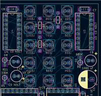
Reason of pending review: the spacing from non-plated hole to trace is smaller than our min 0.2 mm need, and min 0.35 mm need from plated hole to trace.
Suggestion:
Pls expand the spacing to be min 0.2 mm from non-plated hole to trace, and min 0.35 mm from plated hole to trace.