基板クイック試作
カスタム基板試作サービス
基板クイック試作
カスタム基板試作サービス
Last updated: June 2022
Reason of failed review:
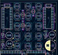
According to our prototype factory's production capability, the diameter of BGA pad (round one below) should be at least 0.25mm, the space between copper trace and BGA PAD should be at least 0.15mm, BGA to Pad should be not less 0.15mm(1OZ complete copper thickness),BGA Pad to BGA Pad should be not less 0.35mm.
PCBWay advanced PCB factory can now manufacturing abilities:
The minimum diameter of BGA is 0.2MM (the sample limit can be 0.15MM), the minimum BGA to line is 3MIL (the prototype limit can be 2.5MIL), the BGA spacing limit is 0.4mm, and the conventional 0.5mm
Challenges to the limit are not easy to produce, because the scrap rate is too high, resulting in increased costs.
Suggestions:
You can update the files and resubmit online for checking again if it’s okay to design according to above capability, but if it’s necessary to make such as 0.2mm BGA or something else over our standard requirements above, it’s free to contact your own sales to quote from our high-tech factory.