基板クイック試作
カスタム基板試作サービス
基板クイック試作
カスタム基板試作サービス
Unused and excessive parts supplied by you or purchased by us will not be returned by default. If you want the parts to be sent back to you with the assembled boards, please contact your service representitive or make a note on your related order, and let us know which parts to send.
リールに供給されていないSMT部品は、1本の連続したテープの上になければなりません。
同じSMT部品を異なるボードに組み立てる必要がある場合は、それらをストリップにカットしないでください。テープの連続ストリップまたはリールに保管してください。
抵抗器、コンデンサ、ダイオード(0603、0805、1206、2225、SOT、SOD、MELF - パッケージ)は最小50個必要で、必要な数量を30個超える必要があります(例:数量40個の組み立て - 必要になります)。 70個 - これは私達の最低50個と組立量の30個以上を満たしています。
抵抗器、コンデンサ、ダイオード(0201、0402、miniMelf、ミニチュアパッケージ)は、最低100個が必要量を50個超えなければなりません(例:組み立て数量80個 - これは最低限130個必要です)。 100個プラス50個以上の組み立て数量)
IC, BGA, QFP,コネクタなどの高価な部品について,少量の余分な(部品の総数に基づく1-5件)を必要とし,それは顺调に组み立てられ,时间通りにあなたの组み立て板を出荷することを确保する。もし質問や質問があれば、私たちにもっと情報を送ったり連絡して回答を獲得してください。
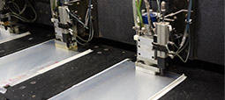
PCBの寸法が50mmx100mmよりも小さい場合、またはPCBが長方形以外の形状(円形または奇数形状)の場合は、ボードを組み立て用にアレイ状にパネル化する必要があります。 パネル化ファイル(はんだペーストデータ)を作成し、パネル化されたPCBに合わせてステンシルを作成するためにデータをPCBA部門に転送します。
ボードの端と銅の部分との間隔が3.5mm(138mil)未満の場合、または何らかの理由でパネルをパネル化する必要がある場合は、2本の長い平行端にブレークアウェイレール(タブ)を追加してください。 ボードが機械によって組み立てられることを確実にするためのボード。
お問い合わせ!
私達のカスタマーサービス+86-571-85317532
The PCBs came out perfectly without any problem very timely!
Quezada
The PCB assembly service exceeded my expectations. Every component was placed accurately and soldered with excellent quality, and the finished boards looked clean and professional. The assembly matched the provided BOM and Pick-and-Place data perfectly, and everything worked as expected after receiving the boards. The production was completed on time, and the overall quality gives me confidence for future prototypes and small production runs. I am very satisfied with the assembly service and would gladly use PCBWay again.
Engineer

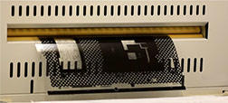
Customer supplied data (gerber) is used to produce the manufacturing data for the specific PCB (artworks for imaging processes and drill data for drilling programs). Engineers compare demands/specifications against capabilities to ensure compliance and also determine the process steps and associated checks. No changes are allowed without PCBWay Group permission.

Artwork Master is PCB production in the key steps, which directly affect the quality of the final product quality,An accurately scaled configuration of electronic data used to produce the artwork master or production master. Artwork Master – The photographic image of the PCB pattern on film used to produce the circuit board, usually on a 1:1 scale.In general, there are three types of Artwork Master:(1) Conductive Pattern (2) solder mask (3) Silkscreen

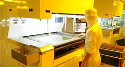
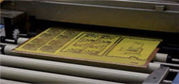
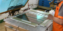
Stage 1 is to transfer the image using an artwork film to the board surface, using photosensitive dry-film and UV light, which will polymerise the dry film exposed by the artwork.
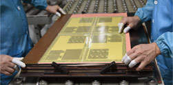
This step of the process is performed in a clean room.
Imaging – The process of transferring electronic data to the photo-plotter, which in turn uses light to transfer a negative image circuitry pattern onto the panel or film.

Stage 2 is to remove the unwanted copper from the panel using etching. Once this copper has been removed, the remaining dry film is then removed leaving behind the copper circuitry that matches the design.
Etching – The chemical, or chemical and electrolytic, removal of unwanted portions of conductive or resistive material.

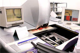
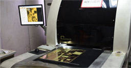
Inspection of the circuitry against digital “images” to verify that the circuitry matches the design and that it is free from defects. Achieved through scanning of the board and then trained inspectors will verify any anomalies that the scanning process has highlighted. PCBWay Group allows no repair of open circuits.

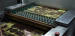
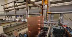
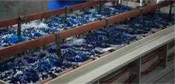
The inner layers have an oxide layer applied and then “stacked” together with pre-preg providing insulation between layers and copper foil is added to the top and bottom of the stack. The lamination process consists of placing the internal layers under extreme temperature (375 degrees Fahrenheit) and pressure (275 to 400 psi) while laminating with a photosensitive dry resist. The PCB is allowed to cure at a high temperature, the pressure is slowly released and then the material is slowly cooled.

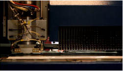
We now have to drill the holes that will subsequently create electrical connections within the multilayer PCB. This is a mechanical drilling process that must be optimised so that we can achieve registration to all of the the inner layer connections. The panels can be stacked at this process. The drilling can also be done by a laser drill

The first step in the plating process is the chemical deposition of a very thin layer of copper on the hole walls.
PTH provides a very thin deposit of copper that covers the hole wall and the complete panel. A complex chemical process that must be strictly controlled to allow a reliable deposit of copper to be plated even onto the non-metallic hole wall. Whilst not a sufficient amount of copper on its own, we now have electrical continuity between layers and through the holes.Panel plating follows on from PTH to provide a thicker deposit of copper on top of the PTH deposit – typically 5 to 8 um. The combination is used to optimise the amount of copper that is to be plated and etched in order to achieve the track and gap demands.

Similar to the inner layer process (image transfer using photosensitive dry film, exposure to UV light and etching), but with one main difference – we will remove the dry film where we want to keep the copper/define circuitry – so we can plate additional copper later in the process.
This step of the process is performed in a clean room.


Second electrolytic plating stage, where the additional plating is deposited in areas without dry film (circuitry). Once the copper has been plated, tin is applied to protect the plated copper.

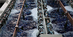
This is normally a three step process. The first step is to remove the blue dry film. The second step is to etch away the exposed/unwanted copper whilst the tin deposit acts an etch resist protecting the copper we need. The third and final step is to chemically remove the tin deposit leaving the circuitry.

Just like with inner layer AOI the imaged and etched panel is scanned to make sure that the circuitry meets design and that it is free from defects. Again no repair of open circuits are allowed under PCBWay demands.

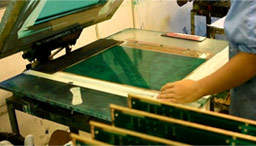
Soldermask ink is applied over the whole PCB surface. Using artworks and UV light we expose certain areas to the UV and those areas not exposed are removed during the chemical development process – typically the areas which are to be used as solderable surfaces. The remaining soldermask is then fully cured making it a resilient finish.
This step of the process is performed in a clean room.

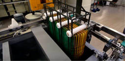
Various finishes are then applied to the exposed copper areas. This is to enable protection of the surface and good solderability. The various finishes can include Electroless Nickel Immersion Gold, HASL, Immersion Silver etc. Thicknesses and solderability tests are always carried out.

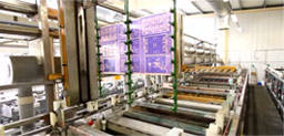
This is the process of cutting the manufac-turing panels into specific sizes and shapes based upon the customer design as defined within the gerber data. There are 3 main options available when providing the array or selling panel – scoring, routing or punching. All dimensions are measured against the customer supplied drawing to ensure the panel is dimensionally correct.

Used for checking the integrity of the tracks and the through hole interconnections – checking to ensure there are no open circuits or no short circuits on the finished board. There are two test methods, flying probe for smaller volumes and fixture based for volumes.We electrically test every multilayer PCB against the original board data. Using a flying probe tester we check each net to ensure that it is complete (no open circuits) and does not short to any other net.

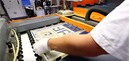
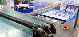
In the last step of the process a team of sharp-eyed inspectors give each PCB a final careful check-over.Visual checking the PCB against acceptance criteria and using PCBWay “approved” inspectors. Using manual visual inspection and AVI – compares PCB to gerber and has a faster checking speed that human eyes, but still requires human verification. All orders are also subjected to a full inspection including dimensional, solderability, etc.

Boards are wrapped using materials that comply with the PCBWay Packaging demands (ESD etcetera) and then boxed prior to be being shipped using the requested mode of transport.