基板クイック試作
カスタム基板試作サービス
基板クイック試作
カスタム基板試作サービス
PCBWay is not only a professional PCB and assembly manufacturing company but also provides customers with high-quality PCB design services. Whether you are innovating in the fields of communications, healthcare, industrial, consumer electronics, or any other industry, our team is ready to help you bring your vision to life.
Our Advantages:
1.Professional Design Team
Our PCB design team consists of experienced engineers who are proficient in design and layout in circuits as well as the best practices of manufacturing and are familiar with a variety of commonly used design software.
2.One-Stop Solution Service:
We provide one-stop solution services, covering the entire process from concept to final product production. This includes shell design, hardware development, software programming, product testing and more.
3. Rapid Design Delivery
Our powerful design capability ensures the shortest possible time on PCB design. For some projects, we can complete your requirements in as little as 24 hours.
4. Manufacturing Advantage
Once the design is complete, we can directly proceed with production at our factory, helping you save a lot of time. Our manufacturing services include 3D&CNC, PCB and assembly.
Reliable PCB design involves not only routing, but also signal integrity, EMI control, thermal management, and manufacturability optimization.
To help engineers better understand modern PCB layout and routing practices, PCBWay also provides a detailed technical guide:
Complete PCB Design Guidelines: Layout, Routing and Manufacturing Best Practices
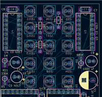
Project Design Examples:

If you are seeking professional PCB design services, we would be honored to assist you.
You can submit your requirements on this page or contact anson@pcbway.com directly
More information please check here: