基板クイック試作
カスタム基板試作サービス
基板クイック試作
カスタム基板試作サービス
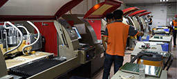
At first sight, PCBs differ little in appearance, irrespective of their inherent quality. It is under the surface that we focus on the differences so critical to the PCBs’ durability and functionality. Customers cannot always see the difference, but they can rest assured that PCBWay puts a great deal of effort into ensuring that in turn, their customers are also supplied with PCBs that meet the most stringent quality standards.Highly Specialized Precision PCBs, & Large Scale Production (No order is too small or too large).our customers achieve the best possible time to market and competitive advantage by producing printed circuit boards in a sustainable way at the lowest total cost through our competence, delivery accuracy and product quality.If you want to see standard PCB or quickturn pcb Capabilities, pls click this link. Advanced PCB Manufacturing Capability,The information below details some of the key capabilities that PCBWay can offer and support today.
| Items | 2016 | 2017 | 2018 | |
|---|---|---|---|---|
| Number of Layers | General PCB board | 2-36 | 2-40 | 2-64 |
| Buried IC | no | yes | yes | |
| HDI(buried and blind vias) | HDI(2+N+2) staggered and stacked vias |
HDI(4+N+4) staggered and stacked vias |
HDI(7+N+7) staggered and stacked vias |
|
| Materials | FR4(shengyi) | yes | yes | yes |
| High Tg | Tg-170 | Tg-210 | Tg-220 | |
| Halogen Free | yes | yes | yes | |
| High Frequency | yes | yes | yes | |
| Maximum board size | 20*30inch(508*762mm) | 20*30inch(508*762mm) | 20*35inch(508*889mm) | |
| Board thickness | 0.21-6.0mm | 0.21-6.0mm | 0.21-6.0mm | |
| Minimum track line | 3mil-inner 3mil-outer | 2mil-inner 3mil-outer | Portion 2mil-inner 2mil-outer | |
| Minimum Spacing line | 3mil-inner 3mil-outer | 2mil-inner 3mil-outer | Portion 2mil-inner 2mil-outer | |
| Outer layer copper thickness | 5oz | 7oz | 8oz | |
| Inner layer copper thickness | 5oz | 7oz | 8oz | |
| Min. finished hole size(Mechanical) | 0.15mm | yes | yes | yes |
| Min. finished hole size(laser hole) | 0.076mm | yes | yes | yes |
| Aspect ratio | 12:1 | 12:1 | 12:1 | |
| Solder Mask Types and brand | NAYA(LP_4G) | yes | yes | yes |
| Tamura(TT19G) | yes | yes | yes | |
| TAIYO(PSR2200) | yes | yes | yes | |
| Solder Mask Color | green;blue;red;white;black | yes | yes | yes |
| Impedance Control Tolerance | ±10%,50Ω and below:±5Ω | yes | yes | yes |
| Plug via hole | Min.size can be plugged: | 0.15mm(CNC)|0.1mm(Laser Blind/buried vias) | 0.15mm(CNC)|0.1mm(Laser Blind/buried vias) | 0.15mm(CNC)|0.1mm(Laser Blind/buried vias) |
| Max.size can be plugged: | 0.7mm | 0.7mm | 0.7mm | |
| Min. annular ring can be kept | 3mil | 3mil | 3mil | |
| Min. distance between the IC pads can keep SM bridge |
8mil | 8mil | 8mil | |
| Min. SM bridge for green soldermask | 3mil | 3mil | 3mil | |
| Min. SM bridge for black soldermask | 4mil | 4mil | 4mil | |
| Surface Treatment | HASL | yes | yes | yes |
| ENIG | yes | yes | yes | |
| OSP | yes | yes | yes | |
| LEAD FREE HASL | yes | yes | yes | |
| GOLD PLATING | yes | yes | yes | |
| IMMERSION Ag | yes | yes | yes | |
| IMMERSION Sn | yes | yes | yes | |
| V-Cut | CNC V-cut, degree | 20\30\45\60 | 20\30\45\60 | 20\30\45\60 |
| V-cut by hand, degree | 20\30\45\60 | 20\30\45\60 | 20\30\45\60 | |
| Outline Profile | CNC | CNC | CNC | |
| Chamfer | The angle typeof the chamfer: | 20\30\45 | 20\30\45 | 20\30\45 |
| Min. distance of jumping chamfer: | 5mm | 5mm | 5mm | |
| Tolerance of the dimension size | ±0.1mm | ±0.1mm | ±0.1mm | |
| Tolerance of the board thickness | 0.21-1.0 | ±0.1 | ±0.1 | ±0.1 |
| 1.0-2.5 | ±7% | ±7% | ±7% | |
| 2.5-6.3 | ±6% | ±6% | ±6% | |
| Tolerance of the finished hole size | 0-0.3mm | ±0.08mm | ±0.08mm | ±0.08mm |
| 0.31-0.8mm | ±0.08mm | ±0.08mm | ±0.08mm | |
| 0.81-1.60mm | ±0.05mm | ±0.05mm | ±0.05mm | |
| 1.61-2.49mm | ±0.075mm | ±0.075mm | ±0.075mm | |
| 2.5-6.0mm | +0.15/-0mm | +0.15/-0mm | +0.15/-1mm | |
| >6.0mm | +0.3/-0mm | +0.3/-0mm | +0.3/-1mm | |
| Certificates(copies are needed) | UL | yes | yes | yes |
| ISO9001 | yes | yes | yes | |
| ISO14000 | yes | yes | yes | |
| ROHS | yes | yes | yes | |
| TS16949 | yes | yes | yes | |
| No. | Item | Process capability parameter | |
|---|---|---|---|
| 1 | Base material | FR-4|High Tg|Halogen-free|PTFE|Ceramic PCB (Scrap rate is too high)|Polyimide | |
| 2 | PCB type | PCB|FPC|R-FPC|HDI | |
| 3 | Max layer count | 64 layers | |
| 4 | Min base copper thickness | 1/3 OZ (12um) | |
| 5 | Max finished copper thickness | 8 OZ | |
| 6 | Min trace width/spacing | Inner layer | 2/2mil (H/H OZ base copper)only part trace with this width and space but not all the board with this trace width and space |
| 7 | Outer layer | 2/2mil (1/3 OZ base copper)only part trace with this width and space but not all the board with this trace width and space | |
| 8 | Min spacing between hole to inner layer conductor | 6mil | |
| 9 | Min spacing between hole to outer layer conductor | 6mil | |
| 10 | Min annular ring for via | 3mil | |
| 11 | Min annular ring for component hole | 5mil | |
| 12 | Min BGA diameter | 8mil | |
| 13 | Min BGA pitch | 0.4mm | |
| 14 | Min hole size | 0.15mm(CNC)|0.1mm(Laser Blind/buried vias) | |
| 15 | Max aspect ratios | 20:1 | |
| 16 | Min soldermask bridge width | 3mil | |
| 17 | Soldermask/circuit processing method | Film|LDI | |
| 18 | Min thickness for insulating layer | 2mil | |
| 19 | HDI & special type PCB | HDI(1-7 steps)|R-FPC(2-16 layers)|High frequency mix-pressing(2-20 layers)|Buried capacitance & resistance …… | |
| 20 | Surface Finish type | ENIG|HAL|HAL lead free|OSP|Immersion Sn|Immersion silver|Plating hard gold|Plating silver | |
| 21 | Max PCB size | 609*889mm | |
| Items | PCB Prototype capacity (area < 1m2;) | Small and medium batch (area > 1m2) | ||
|---|---|---|---|---|
| Materials | General Tg FR4: | shengyi S1141,Kingboard KB6160A | shengyi S1141 | |
| High-Tg Halogen-free: | shengyi S1170G Halogen-free TG170,TU-862 HF TG170 | shengyi S1170G Halogen-free TG170 ,TU-862 HF TG170 | ||
| Medium Tg Halogen-free: | shengyi S1150G Halogen-free TG150 | shengyi S1150G Halogen-free TG150 | ||
| High Halogen-free CTI: | shengyi S1151G( CTI≥600V) | shengyi S1151G( CTI≥600V) | ||
| High CTI: | shengyi S1600( CTI≥600V)Kingboard KB6160C | shengyi S1600( CTI≥600V)Kingboard KB6160C | ||
| Special Material(High low temperature): | shengyi SH260 | shengyi SH260 | ||
| High Tg FR4: | S1000-2, S1000-2M,IT180A | S1000-2, S1000-2M,IT180A | ||
| Ceramic powder filled high frequency | Rogers4003, Rogers4350, Arlon25N,shengyi S7136 | Rogers4350, Rogers4003,shengyi S7136 | ||
| PTFE high frequency material: | Rogers, Taconic, Arlon,Taizhou wangling | Rogers, Taconic, Arlon,Taizhou wangling | ||
| High Frequency PCB PP | RO4450 0.1mm,shengyi Synamic6, | RO4450 0.1mm,shengyi s6 | ||
| High Speed( 1-5G) | MEG4,Tu-862,Tu-662, Tu-768, S7038, S1165, Isola-FR408HR, Isola-FR406,EMC TW -EM370,EM828G IT170GRANP175FM(Nanya) | MEG4, Tu-862, Tu-662, Tu-768,S7038, S1165, Isola-FR408HR, Isola-FR406,EMC TW -EM370, EM828GIT170GRA,NP175FM(Nanya) | ||
| High Speed( 5-10G) | MEG4,Tu-872, N4000-13, M4, Tu-863(Halogen-free),Synamic4, EM-888, I-Speed(Isola) N4800-20SI(Nelco) IT-958G | MEG4,Tu-872, N4000-13, M4, Tu-863(Halogen-free), Synamic4, EM-888, I-Speed(Isola) N4800-20SI(Nelco) IT-958G | ||
| High Speed( 10-25G) | MEG6, Tu-883,shengyi Synamic6, Meteorwave1000/2000/3000(Nelco), EM-891(EMC TW),EM-888K, IT-968, I-Tera MT40(Isola) | MEG6, Tu-883,shengyi Synamic6, Meteorwave1000/2000/3000(Nelco), EM-891(EMC TW), EM-888K, IT-968 I-Tera MT40(Isola) | ||
| High Speed(>25G) | MEG7, Tu-933,Meteorwave4000( Nelco), IT-988, Tachyon 100G(Isola) | MEG7, Tu-933,Meteorwave4000( Nelco), IT-988 Tachyon 100G(Isola) | ||
| High Frequency PCB DK 2.2-2.25 | RO5880, TLY-5(Taconic) SCGA-500 GF220(shengyi), F4BK225 | / | ||
| High Frequency PCB DK 2.33 | RO5870, TLY-3(Taconic) | / | ||
| High Frequency PCB DK 2.45 | TLX-0(Taconic), TLT-0(Taconic) | / | ||
| High Frequency PCB DK 2.5-2.55 | AD250(Arlon), TLT-9(Taconic), TLY-9(Taconic); SCGA-500 GF255(shengyi), TLT-8(Taconic), TLY-8(Taconic), F4B255 | / | ||
| High Frequency PCB DK 2.6-2.65 | TLT-7(Taconic), TLY-7(Taconic); TLT-6(Taconic), TLY-6(Taconic), SCGA-500 GF265(shengyi), F4B265 | / | ||
| High Frequency PCB DK 2.7-2.75 | AD270(Arlon); TLC-27(Taconic) | / | ||
| High Frequency PCB DK 2.92-2.94 | RO6002, CLTE( Arlon) | / | ||
| High Frequency PCB DK 2.95 | AD295(Arlon), TLE-95(Taconic) | / | ||
| High Frequency PCB DK 3.0 | SCGA-500 GF300(AR-320(Arlon), (Taconic), TLC-30(Taconic), RO3203, F4BK300 | / | ||
| High Frequency PCB DK 3.2-3.28 | AD320(Arlon), AR-320(Arlon), TLC-32(Taconic);TMM-3( Rogers);25N(Arlon) | / | ||
| High Frequency PCB DK 3.37-3.38 | 25FR(Arlon), Ro4003 | / | ||
| High Frequency PCB DK 3.48-3.5 | RO4350, RO4835, AR-350(Arlon), RF-35(Taconic), F4BK350 | / | ||
| High Frequency PCB DK 3.6 | AD360(Arlon) | / | ||
| High Frequency PCB DK 4.5 | AR-450(Arlon), TMM-4( Rogers), | / | ||
| High Frequency PCB DK 6.0 | AR-600(Arlon), TMM-6( Rogers), | / | ||
| High Frequency PCB DK 6.15 | RO3006, RO6006, RO4360 | / | ||
| High Frequency PCB DK 9.2-9.8 | TMM-10( Rogers), TMM-101( Rogers) | / | ||
| High Frequency PCB DK 10.0-10.2 | AR-1000(Arlon), CER-10(Taconic), RO3010, RO3210, RO6010 | / | ||
お問い合わせ!
私達のカスタマーサービス+86-571-85317532
The PCBs came out perfectly without any problem very timely!
Quezada
The PCB assembly service exceeded my expectations. Every component was placed accurately and soldered with excellent quality, and the finished boards looked clean and professional. The assembly matched the provided BOM and Pick-and-Place data perfectly, and everything worked as expected after receiving the boards. The production was completed on time, and the overall quality gives me confidence for future prototypes and small production runs. I am very satisfied with the assembly service and would gladly use PCBWay again.
Engineer

顧客提供のデータ(ガーバー)を使用して、特定のPCBの製造データ(イメージングプロセス用のアートワークおよび穿孔プログラム用のドリルデータ)を作成します。 エンジニアは要求/仕様を機能と比較してコンプライアンスを確保し、さらにプロセスステップと関連するチェックを決定します。 PCBWay Groupの許可なしに変更することはできません。


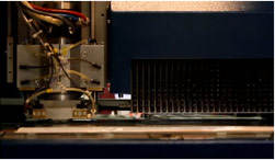
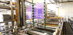
PCB production starts with a large piece of sheet material. Due to the limitations of PCB production equipment and manufacture capabilities, the factory has requirements for its minimum and maximum processing size. Therefore, under the guidance of manufacture instruction (MI), the raw material of PCB (Copper Clad Laminate ) needs to be cut into the processing size by automatic cutting machine before production.
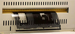

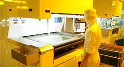
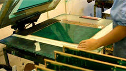
段階1は、アートワークフィルムを用いて感光性ドライフィルムおよびUV光を用いてボード表面に画像を転写することであり、これはアートワークによって露光されたドライフィルムを重合する。 プロセスのこのステップはクリーンルームで行われます。<br> イメージング - 電子データをフォトプロッタに転送するプロセス。フォトプロッタは、光を使用してネガティブ画像回路パターンをパネルまたはフィルムに転送します。

段階2は、エッチングを用いてパネルから不要な銅を除去することである。 この銅が取り除かれると、残りのドライフィルムは取り除かれ、デザインに合った銅回路が残ります。 エッチング - 導電性または抵抗性の材料の不要な部分を化学的、または化学的および電解的に除去すること。


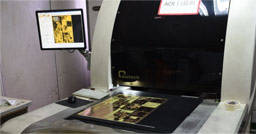
回路が設計と一致し、欠陥がないことを確認するためのデジタル「画像」に対する回路の検査。 ボードのスキャンによって達成され、それから訓練された検査官はスキャンプロセスが強調したどんな異常でも確かめるでしょう。 PCBWayグループは開回路の修理を許可しません。


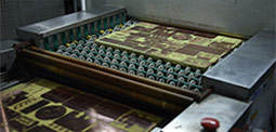
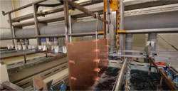
内層には酸化物層が塗布され、次いで層間を絶縁するプリプレグと共に「積み重ね」られ、銅箔が積み重ねの上下に加えられる。 積層工程は、感光性ドライレジストと積層しながら、内層を極端な温度(375°F)および圧力(275から400psi)下に置くことからなる。 PCBを高温で硬化させ、圧力をゆっくり解放し、次いで材料をゆっくり冷却する。

私達は今多層PCBの中で電気接続を後で作成する穴をあけなければならない。 これは、すべての内層接続に対して位置合わせを行うことができるように最適化する必要がある機械的穴あけプロセスです。 この工程でパネルを積み重ねることができる。 穴あけはまたレーザーのドリルによってすることができます

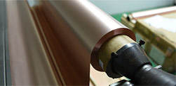
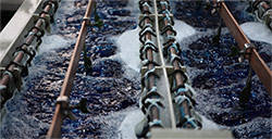
めっきプロセスの最初のステップは、穴の壁に銅の非常に薄い層を化学蒸着することです。
PTHは穴の壁とパネル全体を覆う非常に薄い銅の堆積物を提供します。 信頼性の高い銅の析出物を非金属製の穴の壁にもメッキできるように厳密に制御する必要がある複雑な化学プロセス。 それ自体では十分な量の銅ではないが、我々は今や層間と孔を通して電気的に連続している。パネルめっきはPTH堆積物の上により厚い銅堆積物、典型的には5〜8μmを提供するために続く。 この組み合わせは、トラックおよびギャップの要求を達成するために、メッキおよびエッチングされる銅の量を最適化するために使用されます。

内層プロセス(感光性ドライフィルムを使用した画像転写、UV光への露光、エッチング)と似ていますが、主な違いが1つあります - 銅/定義回路を残したい部分でドライフィルムを削除します。 プロセスの後半で銅。
プロセスのこのステップはクリーンルームで行われます。


追加のめっきがドライフィルム(回路)のない領域に堆積される第二の電解めっき段階。 銅がメッキされると、メッキされた銅を保護するためにスズが塗布されます。
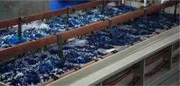

これは通常3段階のプロセスです。 最初のステップは青いドライフィルムを取り除くことです。 2番目のステップは、露出した/不要な銅をエッチング除去する一方で、スズの堆積物が必要な銅を保護するエッチレジストとして機能するようにすることです。 最後の3番目のステップは、回路を離れる錫メッキを化学的に除去することです。

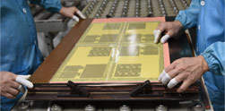
内層AOIの場合と全く同様に、画像形成されエッチングされたパネルは、回路が設計を満たし、それが欠陥がないことを確実にするために走査される。 PCBWayの要求により、開回路の修理はできません。

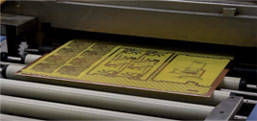
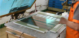
ソルダーマスクインキはPCB表面全体に塗布されます。 アートワークとUV光を使用して、特定の領域をUVにさらし、露光されていない領域(通常ははんだ付け可能な表面として使用される領域)を除去します。 残りのソルダーマスクはそれから完全に硬化されてそれを弾力のある仕上げにする。 プロセスのこのステップはクリーンルームで行われます。

次いで、露出した銅領域に様々な仕上げが施される。 これは表面の保護と良好なはんだ付け性を可能にするためです。 さまざまな仕上げには、無電解ニッケル液浸金、HASL、液浸銀などがあります。厚さとはんだ付け性のテストは常に行われます。

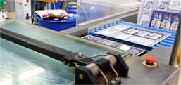
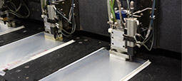
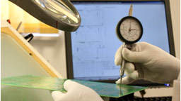
これは、ガーバーデータで定義されている顧客の設計に基づいて、製造パネルを特定のサイズと形状に切断するプロセスです。 配列を提供したりパネルを売ったりするときに利用できる3つの主なオプションがあります - 得点、ルーティングまたはパンチ。 すべての寸法は、パネルの寸法が正しいことを確認するために、お客様から提供された図面に対して測定されます。

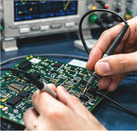
トラックとスルーホールの相互接続の完全性をチェックするために使用されます - 完成したボード上に開回路や短絡がないことを確認するためにチェックします。 2つのテスト方法があります。小体積用のフライングプローブと体積用のフィクスチャです。すべてのPCBを元のボードデータと電気的にテストします。 フライングプローブテスターを使用して、各ネットをチェックして、ネットが完全であり(開回路がない)、他のネットと短絡していないことを確認します。

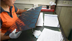
プロセスの最後のステップでは、鋭い目の検査官のチームが各PCBに最終の慎重なチェックオーバーを行います。合格基準に照らしてPCBを視覚的に検査し、PCBWay「承認」検査員を使用します。 手動の目視検査とAVIを使用する - PCBとガーバーを比較し、人間の目より速いチェック速度を持ちますが、それでも人間による検証が必要です。 すべての注文は寸法、はんだ付け性などを含む完全な検査も受けます。

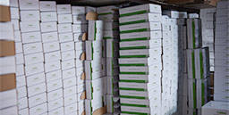
ボードは、PCBWayパッケージング要求(ESDなど)に適合する材料を使用して包装され、要求された輸送モードを使用して出荷される前に箱詰めされます。