基板クイック試作

カスタム基板試作サービス

弊社製プリント基板の例

私達は簡単なものから複雑なベアボードを作るためのPCB製造能力を持っています。
下記のプリント回路例をご覧になり、ご質問がある場合やフォームの見積もりをご希望の場合はお知らせください。

原图
Mouse over to zoom in

20-layer server backplane PCB

Applications
Server field
Features
High speed material + back drill
Material
TU-872
Layers
20 layers
Thickness
5.0±0.5mm
Min Hole Size
/
Min Track/Spacingh
75/75um
Minimum board thickness and hole ratio
12:1
Surface Finish
/
今すぐお見積もり
製品詳細

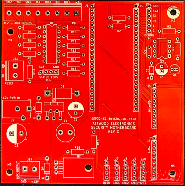
The 20-layer server high-level backplane PCB is made of Tai Yao TU872SLK material and surface immersion gold technology. The PCB circuit board is widely used in data center server PCB backplanes.


Related Products もっと見る >>
  • 24-layer high-density high-speed PCB

    24 layers, Material: TU872SLK, Thickness: 3.2±0.32mm

  • 24-layer high-density aerospace PCB

    24 layers, Material: TU872SLK, Thickness: 3.2±0.32mm

  • 16-layer thick-gold PCB

    16 layers, Material: S1000-2M, Thickness: 6.5mm±0.3mm

  • 16-layer ultra-fine pitch PCB

    16 layers, Material: S1000-2M, Thickness: 2.5±0.25mm

  • 14-layer high-thickness-to-diameter ratio semiconductor test thick gold PCB

    14 layers, Material: S1000-2M, Thickness: 5.0mm±0.5mm

  • 3rd-order 18-layer buried/blind via PCB

    18 layers, Material: S1000-2M, Thickness: 2.1±0.21mm

お問い合わせ!

私達のカスタマーサービス
あなたのPCBの準備ができて

+86-571-85317532

quotesI am impressed with the quality of the boards, the delivery time and responce to all my questions. Best price excellent service and speedy delivery. When I need another board I will certainly use this supplier. "

-Bill Robinson Company

quotesспасибо за платы! платы очень хорошего качества. надежный продавец. оперативно отвечал на вопросы. заказ выполнили и отправили очень быстро.Заказываю платы не в первый раз - как всегда только лучшие впечатления. 5+++. 4 числа отправил файлы 26-го забрал на почте в Москве."

-FVL. SKU Company