基板クイック試作
カスタム基板試作サービス
PCBWay factories will have a holiday off on June 19th. Orders can be placed as usual during holidays, but all orders will be delayed by 1-2 days. Read more >>
基板クイック試作
カスタム基板試作サービス

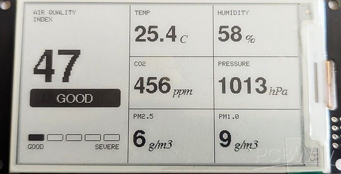
5G signal test PCB board, this type of circuit board is made of RO4350B+TU768 material, produced by mixed pressure, mechanical drilling, surface immersion gold and other processes, the smallest aperture can reach 0.2mm, the Min Track/Spacing can reach 100/100um . The PCB circuit board is widely used in the field of 5G signal testing.


4 layers, Thickness: 1.12mm, Surface Finish: HASL lead free

2 layers, Thickness: 1.2mm

2 layers, Thickness: 1.6mm, Surface Finish: Immersion gold(ENIG)

6 layers, Thickness: 1.6mm, Surface Finish: Immersion gold(ENIG)

6 layers, Thickness: 2.6mm, Size: 6*6cm

10 layers, Material: FR4, Thickness: 1.6mm

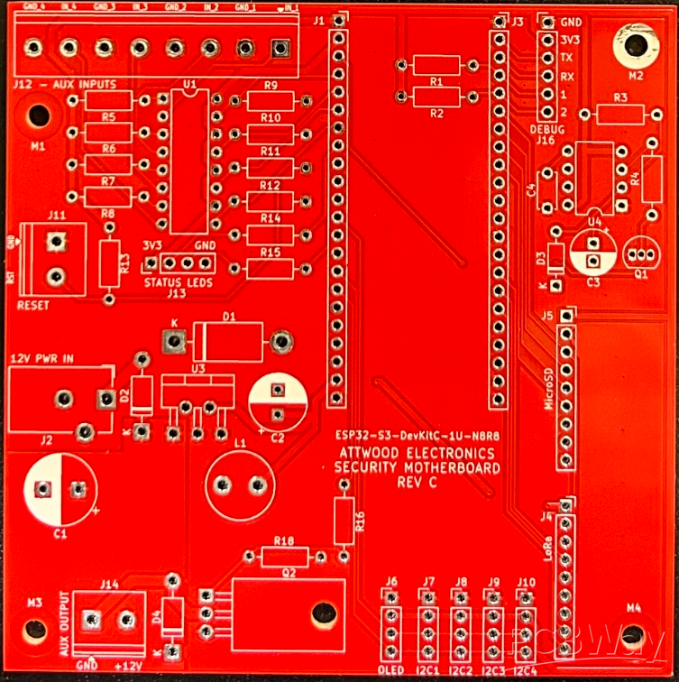
6 layers, Thickness: 1.0mm, Surface Finish: Immersion gold(ENIG) 3U"

12 layers, Material: FR4, Thickness: 1.6mm

4 layers, Thickness: 0.8mm, Surface Finish: Immersion gold(ENIG)

6 layers, Thickness: 1.6mm, Surface Finish: Immersion gold(ENIG)

8 layers, Material: S1000-2M, Thickness: 1.0±0.1mm

12 layers, Material: S1000-2M, Thickness: 1.2±0.1mm