基板クイック試作

カスタム基板試作サービス

弊社製プリント基板の例

私達は簡単なものから複雑なベアボードを作るためのPCB製造能力を持っています。
下記のプリント回路例をご覧になり、ご質問がある場合やフォームの見積もりをご希望の場合はお知らせください。

原图
Mouse over to zoom in

Thick gold semiconductor test PCB

Applications
Semiconductor test
Features
/
Material
S1000-2M
Layers
16 Layers
Thickness
6.5mm±0.3mm
Min Hole Size
Mechanical hole 0.2mm
Min Track/Spacingh
250/250um
Minimum board thickness and hole ratio
14:1
Surface Finish
Immersion gold(ENIG) 0.05um
今すぐお見積もり
製品詳細

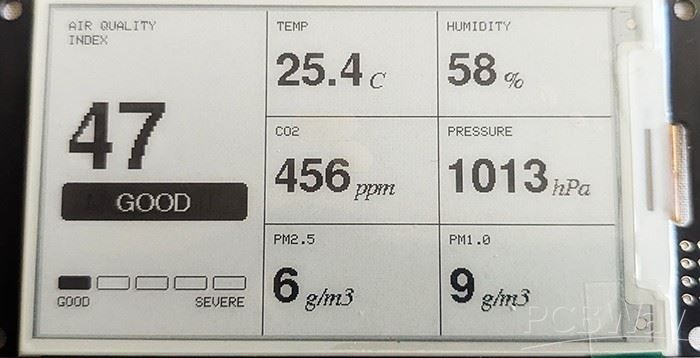
Thick gold semiconductor test PCB boards are mainly used in the field of semiconductor testing. It has a 16-layer structure and uses Shengyi S1000-2M material. The entire board is plated with thick gold.

semiconductor-2-1.jpg

Related Products もっと見る >>
  • Semiconductor test PCB

    8 layers, Material: S1000-2M, Thickness: 4.4±0.4mm

お問い合わせ!

私達のカスタマーサービス
あなたのPCBの準備ができて

+86-571-85317532

quotesI am impressed with the quality of the boards, the delivery time and responce to all my questions. Best price excellent service and speedy delivery. When I need another board I will certainly use this supplier. "

-Bill Robinson Company

quotesспасибо за платы! платы очень хорошего качества. надежный продавец. оперативно отвечал на вопросы. заказ выполнили и отправили очень быстро.Заказываю платы не в первый раз - как всегда только лучшие впечатления. 5+++. 4 числа отправил файлы 26-го забрал на почте в Москве."

-FVL. SKU Company