Holiday Notice: PCBWay factories will be on holiday on May 1st (GMT+8). Orders can be placed as usual during holidays, the delivery date shall be postponed accordingly. Learn more >>

基板クイック試作

カスタム基板試作サービス

弊社製プリント基板の例

私達は簡単なものから複雑なベアボードを作るためのPCB製造能力を持っています。
下記のプリント回路例をご覧になり、ご質問がある場合やフォームの見積もりをご希望の場合はお知らせください。

原图
Mouse over to zoom in

12-layer RF PCB

Applications
Radio frequency antenna
Features
/
Material
RO4350B+TU-768
Layers
12 Layers
Thickness
1.7±0.17mm
Min Hole Size
Mechanical hole 0.2mm
Min Track/Spacingh
110/90um
Minimum board thickness and hole ratio
8.5:1
Surface Finish
Immersion gold(ENIG) 0.05um
今すぐお見積もり
製品詳細

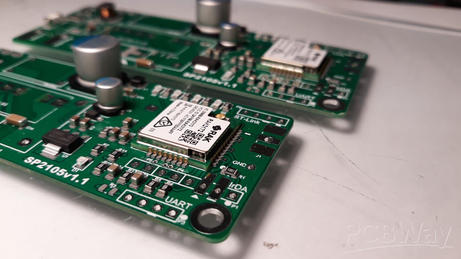
12-layer RF PCB circuit board, using Panasonic R5775G + Lianmao IT180 high-speed materials, mixed pressure, buried resistance and surface immersion gold production technology, as a radio frequency antenna is widely used in the field of communication equipment.

RF antenna PCB board-2-1.jpg

Related Products もっと見る >>
  • 5G RF PCB

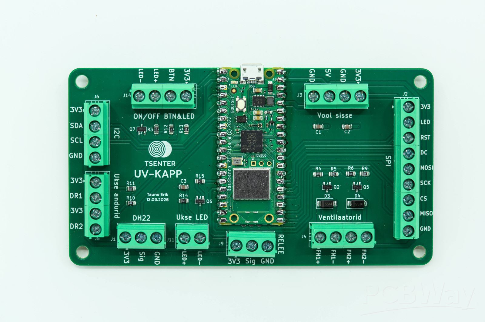
    4 layers, Material: RO4350B+TU768, Thickness: 1.6mm

お問い合わせ!

私達のカスタマーサービス
あなたのPCBの準備ができて

+86-571-85317532

quotesI am impressed with the quality of the boards, the delivery time and responce to all my questions. Best price excellent service and speedy delivery. When I need another board I will certainly use this supplier. "

-Bill Robinson Company

quotesспасибо за платы! платы очень хорошего качества. надежный продавец. оперативно отвечал на вопросы. заказ выполнили и отправили очень быстро.Заказываю платы не в первый раз - как всегда только лучшие впечатления. 5+++. 4 числа отправил файлы 26-го забрал на почте в Москве."

-FVL. SKU Company