基板クイック試作
カスタム基板試作サービス
基板クイック試作
カスタム基板試作サービス

4G optical module PCB circuit boards are widely used in optical fiber communications and other fields. The optical module PCB is made of Shengyi S1000-2M material, surface gold-plated and local thick gold-plated production process, the minimum aperture is 0.15mm, and the minimum line width and line spacing is 120/85um. It is an ideal circuit board for optical fiber communication equipment product.


8 layers, Material: IT968TC, Thickness: 1.0±0.1mm
お問い合わせ!
私達のカスタマーサービス+86-571-85317532
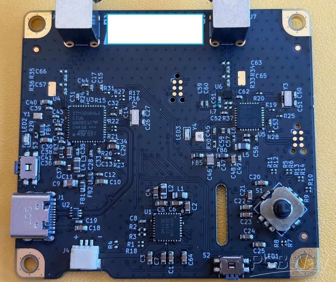
This project is a cold crypto wallet. To have a salesperson work with me directly and to offer such a reasonable price is already good, but the product is just fantastic. I will certainly be back. Thank you guys for your help, I very much look forward to any future business
Engineer
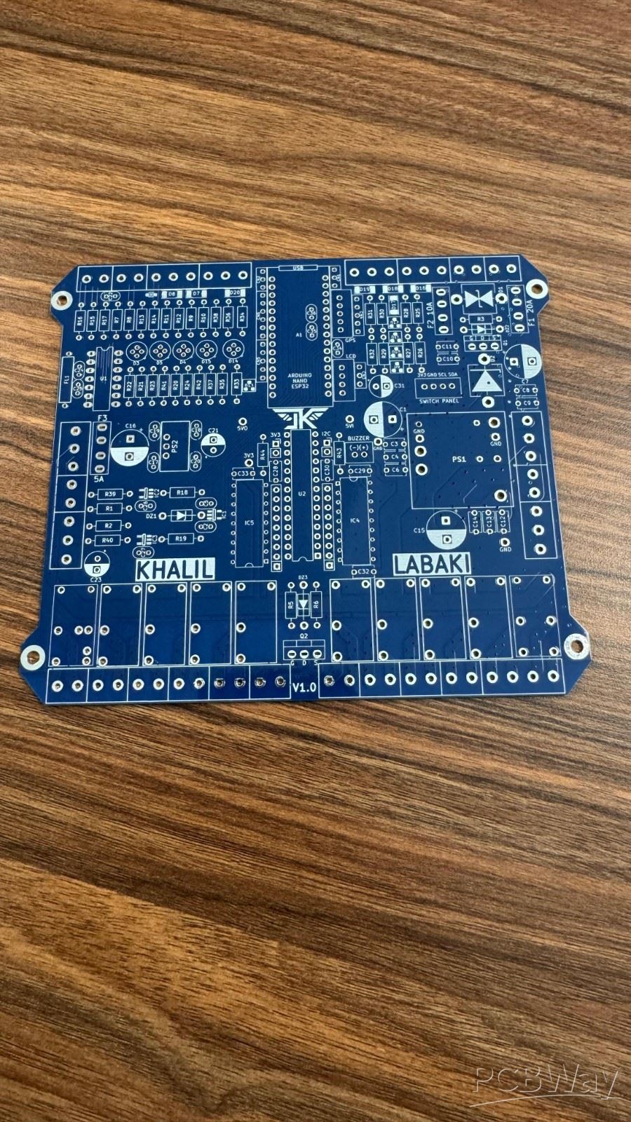
This was my first ever PCB project and my final for computer engineering bachelor's degree. Every day for 2 weeks i've been designing this board, only one shot to get it right. Extremely happy how it turned out.
Kublickas