基板クイック試作
カスタム基板試作サービス
PCBWay factories will have a holiday off on June 19th. Orders can be placed as usual during holidays, but all orders will be delayed by 1-2 days. Read more >>
基板クイック試作
カスタム基板試作サービス

1.1 The circuits should avoid sudden expansion or contraction, and tear shape should be used between the thick and thin circuits.

1.2 The pad should take the maximum value if it meets the electrical requirements. The pad and the conductor are connected by a smooth transition line to avoid a right angle. The independent pad should be padded to enhance the support.


The solid copper foil is designed in the waste area as much as possible.
a) Increase the manual alignment hole to improve the alignment accuracy.
b) The window design considers the scope of the flow glue, usually the window opening is larger than the original design, and the specific size is provided by ME.
c) Small and dense windows can be designed with special molds: rotating, smashing, etc.
a) Smooth transition of the circuits, the direction should be perpendicular to the direction of the bend.
b) The circuits shall be evenly distributed throughout the bending zone.
c) The circuit width should be maximized throughout the bending zone;
d) The joint should try not to adopt the PTH design;
e) Design of Coverlay and No flow PP for joint part.

a) There must be no through holes in the bent part.
b) Add protective copper wire to the outermost side of the circuits. If there is not enough space, choose to add the copper wire at the inner R angle of the bent part.
c) The connecting part of circuits needs to be designed as an arc.
d) The bent area should be as large as possible without affecting the assembly.

The drilling tool of FPC cannot be shared: such as punch holes, ET, SMT positioning holes, etc.


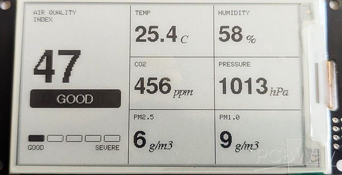
PCB design file errors and solutions