基板クイック試作
カスタム基板試作サービス
基板クイック試作
カスタム基板試作サービス
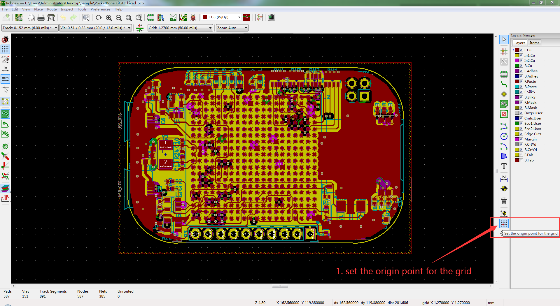
Select the menu bar Place-> Drilling and Position Offset, place the origin at the bottom left corner of the PCB board frame, and then place [Layer Alignment Mark] to the position of the origin just placed.

Click the menu [File] >> [Fabrication Output] >> [Footprint Position (.pos) File], select the output directory, other default, click [Generate Position File]. Open the package location file with Notepad or text editor. You can see the contents have reference number, value, package, X Y coordinate, orientation, board surface, etc.


Check "Generate Gerber Files in Kicad" here - https://www.pcbway.com/blog/help_center/Generate_Gerber_file_from_Kicad.html