In electronic manufacturing, PCBs are vital parts. However, the cost of their manufacturing and assembly is influenced by various factors. From size and materials to specific manufacturing processes utilized, each element you choose significantly impacts the cost. Understanding which factors may lead to price variations can assist you in selecting PCBs that best fit your budget and requirements. Next, we will delve into these factors to help you better comprehend the cost structure of PCB manufacturing and assembly processes.
Delivery Time
- Increased Cost for Urgent Manufacturing: If customers request shorter delivery times, manufacturers may need to work overtime or employ additional shifts to meet delivery requirements. This can result in increased labor costs and production equipment utilization costs, thus leading to higher prices for expedited PCB manufacturing.
- Increased Cost for Special Logistics: For urgent orders, special logistics methods may be necessary to ensure timely delivery, such as air freight or express delivery services. These special logistics services typically come at higher prices, adding extra transportation costs and consequently affecting PCB prices.
- Increased Cost for Production Plan Adjustments: Shorter delivery time requirements may necessitate manufacturers to adjust production schedules and processes to ensure timely order completion. This may involve rearranging production lines, prioritizing certain orders, or accelerating production speeds, thus adding costs associated with production adjustments.
Circuit Complexity
The complexity of the circuit is one of the primary factors influencing PCB costs. As the complexity of the circuit increases, the required number of components also increases, which may lead to higher procurement costs and assembly fees. Additionally, complex circuits may require larger PCB area to accommodate more components and traces, and may also require more layers, all of which further escalate costs.
PCB Size
- Increased Material Costs: Larger PCBs typically require more substrate material and copper foil, which increases material costs. The larger size of the PCB consumes more material, particularly for high-density boards, where the increase in material costs can be significant.
- Increased Manufacturing Complexity: Larger PCBs may necessitate more complex manufacturing processes and larger production equipment, such as larger cutting machines or larger copper plating holes or slots. This increases manufacturing complexity and costs. Additionally, for certain special shapes or sizes of PCBs, additional processing steps or customized processes may be required, further adding to manufacturing costs.
- Increased Shipping Costs: Larger PCBs may incur higher shipping costs. Due to their larger size, larger packaging boxes or additional protective measures may be required to ensure the safe transportation of the products. Additionally, larger PCBs during transportation may incur additional charges, such as oversize cargo fees or higher shipping costs.
Layer Count
- Increased Material Costs: With an increase in the number of layers, the consumption of substrate materials, copper foil, insulation materials, etc., also increases, thus raising material costs.
- Increased Manufacturing Complexity: More layers imply a more complex manufacturing process. In multi-layer PCBs, additional processing steps are required, such as lamination of copper foil layers, drilling, and alignment of inner layer circuitry, which adds to the complexity and difficulty of manufacturing, consequently increasing manufacturing costs.
- Increased Technological Requirements: Multi-layer PCBs typically demand higher levels of manufacturing technology and equipment to ensure precise alignment and connection between each layer, as well as stable signal transmission. This also contributes to increased manufacturing costs.
Substrate Material
- Material Costs: Different types of substrate materials have different material costs. For instance, common FR-4 fiberglass composite materials are typically cheaper compared to high-frequency materials like PTFE. Therefore, choosing different material types directly affects the cost of PCBs.
- Special Performance Requirements: For certain special applications, such as PCBs operating in high-frequency, high-speed, or high-temperature environments, special substrate materials may be required to meet performance requirements. These special substrate materials are typically more expensive. For example, RO4350B is a common high-frequency substrate material with a relatively high price.
- Thickness: The thickness of the substrate material also impacts the price of PCBs. Generally, thicker substrate materials consume more raw materials, resulting in higher costs.
Trace Width and Spacing
- Increased Manufacturing Costs: Smaller trace widths and spacings typically require finer manufacturing processes and higher-level production equipment. For example, smaller trace widths and spacings may necessitate the use of more refined lithography techniques and more precise drilling equipment, which increases manufacturing costs. Additionally, smaller trace widths and spacings may require longer processing times and higher production difficulty, further increasing manufacturing costs.
- Increased Special Process Requirements: Smaller trace widths and spacings may require the adoption of special processes to ensure product quality and performance. For instance, to ensure the accuracy and consistency of trace widths and spacings, stricter inspection and control methods may be necessary, adding additional process requirements and costs.
- Increased Yield Loss: Smaller trace widths and spacings may increase the yield loss during the manufacturing process. Due to the smaller trace widths and spacings, there may be more scrap or defects during production, leading to increased production costs and yield loss. Additionally, because smaller trace widths and spacings may increase the failure rate during manufacturing, extra measures may be required to reduce scrap rates, such as increasing inspection frequency or adjusting production processes, which also adds to manufacturing costs.
Drill Hole Size and Quantity
- Increased Processing Costs: Smaller-sized drill holes typically require the use of more precise drilling equipment and finer drill bits, which increases the difficulty and cost of processing. Additionally, smaller-sized drill holes may require longer processing times and more operational steps, further increasing processing costs.
- Increased Special Process Requirements: For certain specialized PCB requirements, such as blind vias, buried vias, or controlled-depth holes, special drilling processes may be necessary to achieve them. These special processes typically require higher-level processing equipment and more complex operational steps, thus increasing processing costs.
- Increased Material Loss: Drilling processes may result in material loss. A higher quantity of drill holes means more material is cut away and removed, increasing material loss rates. Additionally, for certain specialized PCBs, such as high-density boards, more drill holes may be required to achieve complex circuit layouts, further increasing material loss rates.
Surface Treatment
Different surface treatment methods come with varying costs. For example, HASL (Hot Air Solder Leveling) is relatively inexpensive, while ENIG (Electroless Nickel Immersion Gold) is more expensive. Choosing the appropriate surface treatment method according to requirements can effectively control costs.
Copper Thickness
- Increased Material Costs: Copper foil is one of the fundamental materials of PCBs, and its price is typically calculated based on its thickness. Therefore, thicker copper foil implies a greater quantity of copper material used, thereby increasing material costs.
- Increased Manufacturing Costs: Thicker copper foil usually requires more processing steps and stronger processing equipment to ensure processing quality. For example, during the drilling process, thicker copper foil may require more durable drill bits, and during the chemical etching process, more etching time and stronger chemical concentrations may be necessary. These increased processing requirements lead to higher manufacturing costs.
Hidden Costs of PCBs
While the factors mentioned earlier may significantly impact the price of PCBs, there are also some often overlooked hidden costs to consider.
- Prototype Fabrication and Testing Costs:
Before PCB manufacturing, prototyping and testing must be conducted to ensure compliance with design specifications and requirements. This process can consume a considerable amount of time and funds, as multiple iterations are typically needed to achieve the desired results.
- Assembly and Testing Costs:
After manufacturing, PCBs need to undergo assembly and testing to ensure their proper functioning. This process can be time-consuming and expensive, especially if the PCB requires special assembly techniques or testing procedures.
- Quality Control and Certification Costs:
Extra testing and certification may be required to ensure that PCBs meet quality standards. This may include environmental testing, electrical testing, and safety certification. These additional processes can quickly escalate costs, especially if the PCB requires multiple certifications.
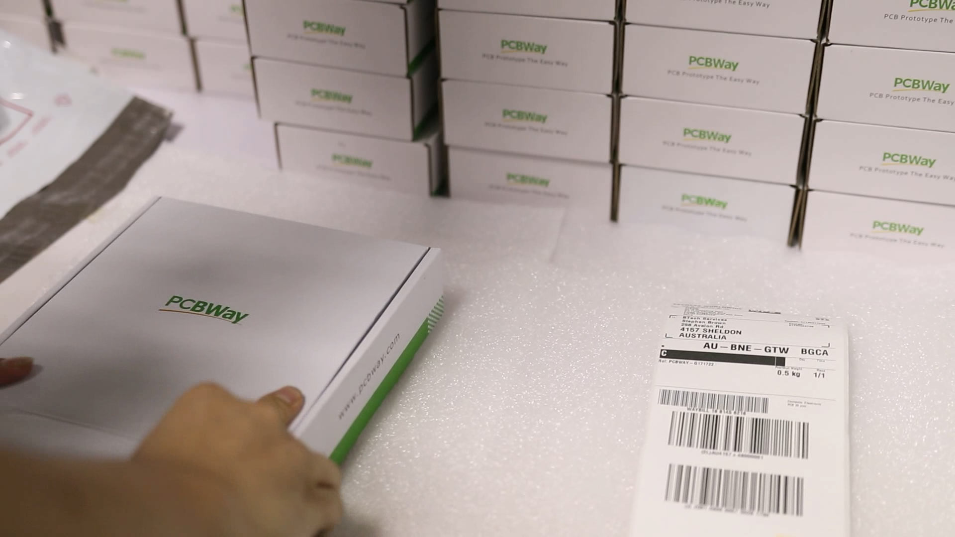
- Transportation and Logistics Costs:
Transportation and logistics costs are also factors to consider. This includes shipping PCB materials to the manufacturing facility, delivering finished PCBs to customers, and any additional handling or storage fees that may be involved.
How to Reduce PCB Manufacturing and Assembly Costs?
- Simplify Circuit Design: Simplifying circuit design is an effective method to reduce the cost of custom PCBs. A simplified design means fewer components, thereby lowering procurement and assembly costs. Additionally, simplifying the design may reduce the number of layers, further reducing material and processing costs.
- Reduce Layer Count: As mentioned earlier, the number of layers in a PCB significantly impacts costs. By reducing the layer count, material and processing costs can be lowered, thus reducing overall costs.
- Use Standard Components: Using standard components can lower the cost of custom PCBs. Standard components are readily available and typically lower in cost compared to specialized components. Furthermore, using standard components helps simplify the design and reduces the required number of layers.
- Optimize PCB Size and Shape: Optimizing the size and shape of the PCB also helps reduce costs. Smaller PCBs require less material and processing, thus reducing manufacturing costs. Additionally, PCBs with simpler shapes may require fewer processing steps, further reducing costs.
- Apply Design for Manufacturability (DFM) Principles: DFM principles are a set of principles for optimizing product design for efficient and cost-effective manufacturing. By applying DFM principles to PCB design, manufacturing costs can be reduced while improving the quality and reliability of the final product. For example, using appropriate line widths and spacings, reducing the number of drill holes, etc., can significantly lower production costs.


