基板クイック試作
カスタム基板試作サービス
基板クイック試作
カスタム基板試作サービス
PCBWayは、シンセン市にあるプロのクイックターンPCBプロトタイピング、PCBアセンブリおよび少量生産メーカーです(3つの主要PCBと2つのPCBアセンブリ生産)。
以下の情報は、PCBWayが今日提供しサポートすることができる主な機能のいくつかを詳述しています。 あなたがここで私たちがサポートできる特定の材料、私たちが現在生産しているPCB技術や製品タイプ、そして私たちが達成できる公差のいくつかに関する情報を見つけるでしょう。
最初のカテゴリーは、私たちが「クイックターン」と呼んでいるもので、少量 - クイックターンPCB、カスタムスペック - クイックターンPCBを提供できることを意味します。
2つ目は、当社の「アドバンスト」製品で、これはPCBWayが提供できる最高のものを示しています。フルスペックPCB、高度に特殊化された精密PCB、および大規模生産です。
あなたのボードが下記の能力を超えているならば、あなたのセールス担当者にメッセージを送ってください。
“スタンダード基板” = アドバンスト + クイックターン
| Items | Manufacturing Capabilities | Remarks | |
|---|---|---|---|
| Number of Layers | - | 1-10 layers | For orders above 10 layers,please view the below "Standard PCB" or contact our sales rep. |
| Material | - |
FR-4,Aluminum
|
For Flex, Rigid-flex, Metal-based (Aluminum etc.,), HDI, Halogen-free, High Tg, etc.,please view the below "Standard PCB" or contact sales rep. |
| Maximum PCB Size(Dimension) | - | 500*1100mm (min 5*6mm) | Any sizes beyond this dimension, please view the below "Standard PCB" or contact sales rep. |
| Board Size Tolerance(Outline) | - | ±0.2mm/±0.5mm | ±0.2mm for CNC routing, and ±0.5mm for V-scoring. |
| Board Thickness |  |
0.2-2.4mm | 0.2,0.4, 0.6, 0.8, 1.0, 1.2, 1.6, 2.0, 2.4mm. Please view the below "Standard PCB" or contact us if your board exceeds these. |
| Board Thickness Tolerance(t≥1.0mm) | - | ±10% | Normally “+ Tolerance” will occur due to PCB processing steps such as electroless copper, solder mask and other types of finish on the surface. |
| Board Thickness Tolerance(t<1.0mm) | - | ±0.1mm | |
| Min Trace |  |
0.1mm/4mil | Min manufacturable trace is 4mil(0.1mm), strongly suggest to design trace above 6mil(0.15mm) to save cost. |
| Min Spacing | Min manufacturable spacing is 4mil(0.1mm), strongly suggest to design spacing above 6mil(0.15mm) to save cost. | ||
| Outer Layer Copper Thickness |  |
1oz/2oz/3oz(35μm/70μm/105μm) | Also known as copper weight. 35μm=1oz, 70μm=2oz, 105μm=3oz. Please view the below "Standard PCB" or contact us if you need copper weight greater than 3oz. |
| Inner Layer Copper Thickness |  |
1oz/1.5oz(35μm/50μm) | Inner copper weight as per customer’s request for 4 and 6 layers(Multi-layer laminated structure). Please contact us if you need copper weight greater than 1.5oz. |
| Drill Sizes (CNC) |  |
0.2-6.3mm | Min drill size is 0.2mm, max drill is 6.3mm. Any holes greater than 6.3mm or smaller than 0.3mm will be subject to extra charges. |
| Min Width of Annular Ring |  |
0.15mm(6mil) | For pads with vias in the middle, Min width for Annular Ring is 0.15mm(6mil). |
| Finished Hole Diameter (CNC) |  |
0.2mm-6.2mm | The finished hole diameter will be smaller than size of drill bits because of copper plating in the hole barrels |
| Finished Hole Size Tolerance(CNC) | - | ±0.08mm | For example, if the drill size is 0.6mm, the finished hole diameter ranges from 0.52mm to 0.68mm will be considered acceptable. |
| Solder Mask |  |
LPI | Liquid Photo-Imageable is the mostly adopted. Thermosetting Ink is used in the inexpensive paper-based boards. |
| Minimum Character Width(Legend) |  |
0.15mm | Characters of less than 0.15mm wide will be too narrow to be identifiable. |
| Minimum Character Height (Legend) | - | 0.8mm | Characters of less than 0.8mm high will be too small to be recognizable. |
| Character Width to Height Ratio (Legend) | - | 1:5 | In PCB silkscreen legends processing, 1:5 is the most suitable ratio |
| Minimum Diameter of Plated Half Holes | - | 0.6mm | Design Half-Holes greater than 0.6mm to ensure better connection between boards. |
| Surface Finishing |  |
HASL with lead HASL lead free Immersion gold,OSP |
The most popular three types of PCB surface finish. Please view the below "Standard PCB" or contact us for other finishes. |
| Solder Mask |  |
Green ,Red, Yellow, Blue, White ,Black |
No extra charge (Green, Red, Yellow, Blue) |
| Silkscreen | |
White, Black, None |
No extra charge. |
| Panelization |  |
V-scoring, Tab-routing, Tab-routing with Perforation (Stamp Holes) |
Leave min clearance of 1.6mm between boards for break-routing. For V-score panelization, set the space between boards to be zero. |
| Others | - | Fly Probe Testing (Free) and A.O.I. testing(free), ISO 9001:2008 ,UL Certificate |
No extra charge. |
| Categories | No. | Items | PCB process parameters | Remarks | |||||
|---|---|---|---|---|---|---|---|---|---|
| Normal process | Medium difficulty | High difficulty | |||||||
| Non-standard review | Unable to make | ||||||||
| product type | 1 | Multilayer PCB Layers | 3L≤Layers≤16L | 18L≤Layers≤24L | ≥24L | ||||
| 2 | Blind and Buried Vias | HDI(1+1+....+N+......+1+1) | Anylayer HDI | HDI(2+...+N...+2) | If meet the requirements of 2, 6, and 21 at the same time, it is classified as a high requirement product (thickness to diameter ratio, copper thickness of hole) | ||||
| 3 | Surface Coating | HASL(+gold finger),immersion gold, Immersion Gold +gold fingers with hard gold,OSP (+gold finger with hard gold), Immersion Tin (+gold finger with hard gold) (Not two different surface finish),Immersion Tin | Local immersion gold (long or short gold fingers, segmented gold finger craft) | Exceed this range require unconventional production processes | Partial immersion gold, thickness of gold or nickel reference to the thickness of the coating | ||||
| 4 | Board Material | FR-4;aluminum,Rogers4 series + FR-4 mixed(The Prepreg is ShengYi brand and ROGERS4403 series);CEM-3、LianMao IT158/IT180A | Pure ROGERS4 series multi-layer board (Prepreg is 4450F),PTFE、aluminum+FR4、PTFE+FR4 | Exceed this range require unconventional production processes | Pure PTFE multi-layer board | Pure PTFE can’t be made because the lamination temperature isn’t up to standard,Can‘t laminate Rogers copper foil directly | |||
| Drills | 5 | Drill diameter | Nc drill | 0.20mm≤Drill diameter≤6.5mm More than 6.0mm using CNC milling hole diameter 0.2mm: maximum board thickness 1.6mm hole diameter diameter 0.25mm:maximum board thickness 2.0mm, hole diameter 0.3mm≤Ф≤0.35mm, maximum board thickness 3.2 mm, hole diameter 0.4mm≤Ф≤0.55mm, maximum board thickness 4.8 mm, hole diameter>0.55mm maximum board thickness 6.4 mm |
6.5mm or more ±0.1mm ≤ hole diameter tolerance (using CNC milling for 6.5mm or more) | The drill diameter more than 6.0mm, the hole diameter tolerance less than ±0.1mm. If exceed this range require unconventional production processes | Drill diameter below 0.2mm, and the aspect ratio≥10, which is medium difficulty | ||
| 6 | Thickness to diameter ratio | Thickness to diameter ratio≤8 | 8| 10 | Thickness to diameter ratio greater than 12 when the aperture cannot be compensated |
If need to meet the requirement of 2, 6, and 21, it will be treat as high requirement product. |
| |||
| 7 | countersink | hole diameter | 3.0mm≤hole diameter≤6.5mm | Unconventional production beyond this range | Countersink depth tolerance is controlled 0.15mm | ||||
| Angle | 90° | Unconventional production beyond this range | |||||||
| 8 | Hole position tolerances | ±0.075mm | ±0.05mm | <+/-0.05mm | |||||
| 9 | hole diameter tolerance | PTH | ±0.075mm or no customer requirements | ±0.05≤ hole diameter tolerance <±0.75mm | <±0.05mm | <+/-0.05mm | Metallized hole diameter tolerance of 6.0mm or more refers to the requirement of serial number 5 | ||
| NPTH | ≥±0.075mm | <±0.05mm | <+/-0.025mm | ||||||
| Special hole | pressfit | ≤±0.05 | \ | \ | |||||
| non-plated Countersink/Counterbore holes(NPTH) | hole diameter <10mm:tolerance ±0.15mm,hole diameter ≥10mm:tolerance ± 0.20mm | \ | \ | ||||||
| non-plated Countersink/Counterbore holes(NPTH) | hole diameter <10mm:tolerance ±0.2mm hole diameter ≥10mm:tolerance+0.3mm |
\ | \ | ||||||
| 10 | Hole to hole spacing | component hole | ≥16MIL | 14≤Hole to hole spacing≤16 | 13≤Hole to hole spacing≤14 | <13mil | |||
| via(≤0.45mm) | ≥11MIL | ||||||||
| 11 | Slot (Cut-out) | Slot width | Plated slot ≥0.5mm Non-plated slot ≥0.8mm |
\ | \ | More than 1.0mm, can be slot by machine | |||
| Length to width ratio of slot | Length to width≥2 | Length to width<2 | |||||||
| 12 | Castellated Holes | Castellated Holes diameter | ≥0.5mm | 0.5mm>diameter≥0.4mm | \ | ||||
| Castellated Holes spacing (edge to edge) | ≥0.3mm | 0.3mm>diameters≥0.2mm | \ | ||||||
| 13 | Minimum isolation ring of Inner layer, The distance between minimum hole in Inner layer and circuit (before compensation) |
4L | ≥7MIL | 6MIL≤isolation ring, distance<7MIL | 5MIL≤isolation ring, distance<6MIL | If the size of one side is greater than 600MM, the inner hole to line and the hole to copper spacing must be greater than or equal to 15mil. If less than 15mil, it must be treated as unconventional review. The conventional process of 10 layers or more need to be incremented by 1 mil for each additional 2 layers. Change the isolation ring to 12mil or more as much as possible | |||
| 6L | ≥8MIL | 6.5MIL≤isolation ring, distance<8MIL | 6MIL≤isolation ring, distance<6.5MIL | ||||||
| 8L | ≥9MIL | 7MIL≤isolation ring, distance<9MIL | 6MIL≤isolation ring, distance<7MIL | ||||||
| ≥10L | ≥10MIL | 8MIL≤isolation ring, distance<10MIL<9MIL | 7MIL≤isolation ring, distance<8MIL | ||||||
| image transfer | 14 | The min width/spacing of inner layer (before compensation) | copper thickness 18um | ≥4/4 mil | ≥4/3.5 mil | <3.5/3 mil | width/spacing | ||
| copper thickness 35um | ≥4/5 mil | ≥4/4 mil | <3.5/4 mil | width/spacing | |||||
| copper thickness 70um | ≥6/8mil | ≥6/7mil | <5/6 mil | width/spacing | |||||
| copper thickness 105um | ≥8/11 mil | ≥8/10 mil | <6/9 mil | width/spacing | |||||
| 15 | The min width/spacing of outer layer (before compensation) | copper thickness 18um | ≥4/5 mil | ≥4/4 mil or parts 3.5/3.5mil | <3.5/3.5 mil | Local 3.5/3.5mil, only the distance from the GBA chip area line to the PAD | |||
| copper thickness 35um | ≥5/6 mil | ≥5/5 mil | <4/4 mil | ||||||
| copper thickness 70um | ≥7/8mil | ≥6/7mil | <5/6 mil | ||||||
| copper thickness 105um | ≥10/12 mil | ≥8/10 mil | <6/9 mil | ||||||
| 16 | grid trace width/spacing | copper thickness 18um | ≥7/9 mil | ≥6/8 mil | <6/7 mil | ||||
| copper thickness 35um | ≥9/11 mil | ≥8/10 mil | <8/9 mil | ||||||
| copper thickness 70um | ≥11/13mil | ≥10/12mil | <10/11 mil | ||||||
| copper thickness 105um | ≥13/15 mil | ≥12/14 mil | <12/13 mil | ||||||
| 17 | Minimum weld ring (outer layer) | copper thickness 18um | via hole | ≥5mil | ≥4mil | <3 mil | |||
| component hole | ≥8mil | ≥6mil | <6 mil | ||||||
| copper thickness 35um | via hole | ≥5mil | ≥4mil | <3 mil | |||||
| component hole | ≥10mil | ≥8mil | <8 mil | ||||||
| copper thickness 70um | via hole | ≥7mil | ≥6mil | <5 mil | |||||
| component hole | ≥12mil | ≥10mil | <10 mil | ||||||
| copper thickness 105um | via hole | ≥8mil | ≥6mil | <6 mil | |||||
| component hole | ≥14mil | ≥12mil | <12 mil | ||||||
| 18 | width tolerance | width tolerance:≥±20% | ±10%≤ width tolerance:<±20% | <±10% | spacing must meet the requirements of 11 and 12, lf width is greater than 15mil, controlled by ±2.5mil | ||||
| BGA pad diameter | hot air leveling (original) | ≥12MIL | ≥10MIL | <8mil | |||||
| immersion gold (original) | diameter≥11mil | 8.0mil≤diameter<11.0mil | <6mil | ||||||
| 19 | Line to board edge distance | CNC milling | 0.25mm | 0.20mm | <0.20mm | ||||
| SMT width | ≥12mil | ≥9mil | <9mil以下 | <7mil,except the binding board | |||||
| Metal plating | 20 | Plating Thickness(µin) | Electroless Nickel-Immersion Gold,ENIG | Nickel thickness | 100-150 µin | 200 µin | |||
| gold thickness | 1-8 µin | >8 µin | |||||||
| Full board gold plating | Nickel thickness | 100-150 µin | 200-500 µin | Order center check the final price | |||||
| gold thickness | 1-10 µin | 10-50 µin | >50 µin | ||||||
| gold finger | Nickel thickness | 120-150 µin | 200-400 µin | ||||||
| gold thickness | 1-30 µin | 30-50 µin | >50 µin | ||||||
| 21 | Hole copper thickness (µm) | Through hole | 18-25 µm | 30-50 µm | >50 µm | If 2,6,19 is required to exist at the same time, it will be treated as high requirement. The thickness of the copper is 25-50UM, and the thickness of the copper is required to be 2-3OZ generally. | |||
| Blind hole (mechanical hole) | 18-25 µm | 30-50 µm | >50 µm | ||||||
| Buried hole | 15-25 µm | 30-50 µm | >50 µm | ||||||
| 22 | Bottom copper thickness | Inner and outer copper thickness (OZ) | 0.5-4 | 4-6 | >6 | ||||
| solder mask | 23 | solder mask | green solder mask opening(mil) | ≥2mil | 1.5 | 1 | 1mil is only concentrated in the BGA area. If the window can be enlarged, increase it as much as possible, but the maximum is 3mil | ||
| green solder mask Bridge(mil) | copper thicknesss<2OZ | 4(spacing between ICs is 8 mil, green oil),variegated or black oil≥4.5mil | 3-4(spacing between ICs is 7-8 mil, green oil),variegated or black oil≥4mil | ||||||
| copper thicknesss≥2OZ | 5 | 4 | |||||||
| Plug Hole diameter | 0.20mm≤hole diameter≤0.40mm,plug hole fullness 70% | 0.4mm< hole diameter ≤0.70mm | fullness 100% | ||||||
| Plug Hole board thickness | 0.40mm≤board thickness≤2.4mm | >2.4MM | |||||||
| 24 | solder mask | solder mask color | Green, matt green, blue, red, black, matte black, white, yellow | \ | \ | Special colors need to be purchased or deployed in advance | |||
| silkscreen | 25 | Etched silkscreen (finished copper thickness) | Copper thickness 18um | word width/word height | 8MIL/40MIL | 7MIL/35MIL | |||
| Copper thickness 35um | word width/word height | 9MIL/40MIL | 8MIL/35MIL | ||||||
| Copper thickness 75um | word width/word height | 12MIL/60MIL | 10MIL/50MIL | ||||||
| Copper thickness 105um | word width/word height | 16MIL/60MIL | 14MIL/50MIL | ||||||
| outline | 26 | Maximum board thickness | Double PCB | 3.2MM | 4.5MM | >4.5MM | calculated by 4 layers if the thickness more than 3mm | ||
| Multilayer layer board | 3.2MM | 4.5MM | >4.5MM | ||||||
| 27 | Minimum board thickness (single and double panel refers to substrate thickness) | Single or Double side PCB (pcb prototype) | ≥0.3mm | 0.25mm | |||||
| 4L | ≥0.60mm | 0.40mm | <0.40mm | ||||||
| 6L | ≥0.9mm | 0.70mm | <0.70mm | ||||||
| 8L | ≥1.20mm | 1.00mm | <1.00mm | ||||||
| 10L | ≥1.40mm | 1.20mm | <1.20mm | ||||||
| 12L | ≥1.70mm | 1.50mm | <1.50mm | ||||||
| 14L | ≥2.00mm | 1.80mm | <1.80mm | ||||||
| 28 | thickness (T) tolerance MM (multilayer layer pcb) | T≤1.0 | ±0.10 | Need to review if less than the tolerance | If the tolerance is unilateral tolerance, the tolerance shall be double tolerance value, such as: 1.8mm requires positive tolerance, the tolerance shall be 0-0.36mm | ||||
1.0| ±0.13 |
| | |||||||
1.6| ±0.18 |
| | |||||||
2.5| ±0.23 |
| | |||||||
| T≥3.2 | ±8% | ||||||||
| 29 | Maximum finished board size | Single and double side PCB | 508×610mm | Beyond this range needs to be reviewed | |||||
| Multilayer Layer PCB | 508×600mm | ||||||||
| 30 | Minimum finished pcb size | ≥20mm | 10mm≤Size<20mm | <10mm | |||||
| 31 | Beveling for gold finger | Bevel angle | 20°30°45°60° | <20°Or>60° | |||||
| Bevel angle tolerance | >±5° | ±5° | <±5° | ||||||
| Bevel depth tolerance | tolerance≥±0.15mm | ±0.15mm< Tolerance ≤ ±0.1mm | tolerance<±0.10mm | ||||||
| 32 | Shape tolerance | tolerance≥±0.15mm | ±0.10mm≤tolerance<±0.15mm | Tolerance<±0.10mm or more than two form tolerance control | |||||
| 33 | V-CUT | Angle | 20°30°45°60° | ||||||
| The Maximum number of V-CUT | In 20 times | In 30 times | In 40 times | ||||||
| Width of the shape | 80MM< width <560MM | 60MM< width <80MM | width <60MM | ||||||
| board thickness | 0.6MM≦thickness≦2.4MM | 0.5MM≦thickness<0.6MM | thickness<0.5MM or thickness>2.4MM | below 0.5mm is single-sided V-CUT | |||||
| Remaining thickness | ≥0.25MM | <0.25MM | |||||||
| V-CUT | Conventional V-CUTT、V-CUT: Skip V-CUT | \ | \ | ||||||
| others | 34 | panel size | The minimum panel size | ≥100*120mm | \ | <100*120mm | The thickness of the finished board is less than 0.4MM, the panel size can’t exceed 14inch, and the maximum size of the HASL PCB can’t exceed 24inch | ||
| the Maximum panel size | ≤20*24 inch | \ | Need to review if beyond range | ||||||
| 35 | impedance control | Impedance control tolerance | ±10%,50Ω and below:±5Ω | \ | <±10%,50Ω and below <±5Ω | ||||
| bow and twist | bow and twist tolerance | bow and twist≤0.75% | 0.5%≤bow and twist≤ 0.75% | bow and twist<0.5% | asymmetry boards bow and twist tolerance 1.2% | ||||
| 36 | HASL processing capacity | component hole diameter | hole diameter>0.5mm | 0.4mm≤hole diameter≤0.5mm | |||||
| board thickness | 0.5mm≤board thickness≤3.5mm | 0.4mm≤board thickness<0.5mm | |||||||
| thickness | 2um≤thickness of Tin≤30um | \ | \ | ||||||
| 37 | Acceptance Criteria | IPC standard | IPC2 level standard | IPC Level 3 standard | |||||
私達のPCBの機能を見直してくれてありがとう。 あなたが私たちのオンライン購入手続きを通過するとき、ガーバーファイル、.pcb、.pcbdocまたは.camファイルのフォーマットであなたのPCBファイルをアップロードしてください。 ガーバーファイルを提供するために最善を尽くしてください。 しかし、あなたが(.pcb / .pcbdoc)フォーマットのDXPファイルしか持っていないならば、我々はgerberに転送するためにALtium Designer23.21 or 10.0ソフトウェアを使います。それで、AD23.21 or 10.0より高いバージョンを避けてください。 しかし、我々はあなたがウェブページでオンラインで注文することを強く勧めます。


 Smart Devices: 私たちはこれらの業界に大きな顧客基盤を持っています。 試作および製造段階でお客様のPCBを製造することをお客様が選択しています。
 医学: 医学および生物医学の顧客は私達の顧客の大部分を占めます。 私達に厳密な品質規格および短い調達期間があり、私達の価格は競争です、この分野の私達の顧客基盤はまだ上昇しています。
 商業用、工業用および自動車用:
私達の顧客のほとんどはこれらの産業にあります。 迅速な対応、短納期、専門的な技術サポートの継続的に手頃な価格は、これらの業界における顧客規模の維持と拡大に役立ちます。
商業用、工業用および自動車用:
私達の顧客のほとんどはこれらの産業にあります。 迅速な対応、短納期、専門的な技術サポートの継続的に手頃な価格は、これらの業界における顧客規模の維持と拡大に役立ちます。
 大学、学校、そしてアマチュア:
学生は私たちの将来の科学者です、私たちは彼らをサポートします! 学生とアマチュアは価格に敏感な顧客です、我々は彼らが価格と品質に関して彼らのPCBニーズのために我々に頼るであろうという我々の価格保証! 同時に、私たちの教育スポンサーシッププログラムは無料のPCBを大学生に提供しています。あなたのプロジェクトまたは競争の詳細をservice25@pcbway.com に送ってください。
大学、学校、そしてアマチュア:
学生は私たちの将来の科学者です、私たちは彼らをサポートします! 学生とアマチュアは価格に敏感な顧客です、我々は彼らが価格と品質に関して彼らのPCBニーズのために我々に頼るであろうという我々の価格保証! 同時に、私たちの教育スポンサーシッププログラムは無料のPCBを大学生に提供しています。あなたのプロジェクトまたは競争の詳細をservice25@pcbway.com に送ってください。
お問い合わせ!
私達のカスタマーサービス+86-571-85317532
 I am impressed with the quality of the boards, the delivery time and responce to all my questions. Best price excellent service and speedy delivery. When I need another board I will certainly use this supplier. "
спасибо за платы! платы очень хорошего качества. надежный продавец. оперативно отвечал на вопросы. заказ выполнили и отправили очень быстро.Заказываю платы не в первый раз - как всегда только лучшие впечатления. 5+++. 4 числа отправил файлы 26-го забрал на почте в Москве."

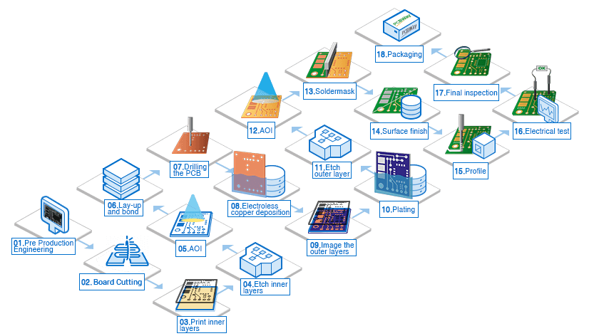
顧客提供のデータ(ガーバー)を使用して、特定のPCBの製造データ(イメージングプロセス用のアートワークおよび穿孔プログラム用のドリルデータ)を作成します。 エンジニアは要求/仕様を機能と比較してコンプライアンスを確保し、さらにプロセスステップと関連するチェックを決定します。 PCBWay Groupの許可なしに変更することはできません。


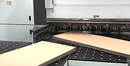
PCB production starts with a large piece of sheet material. Due to the limitations of PCB production equipment and manufacture capabilities, the factory has requirements for its minimum and maximum processing size. Therefore, under the guidance of manufacture instruction (MI), the raw material of PCB (Copper Clad Laminate ) needs to be cut into the processing size by automatic cutting machine before production.

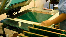
段階1は、アートワークフィルムを用いて感光性ドライフィルムおよびUV光を用いてボード表面に画像を転写することであり、これはアートワークによって露光されたドライフィルムを重合する。 プロセスのこのステップはクリーンルームで行われます。
イメージング - 電子データをフォトプロッタに転送するプロセス。フォトプロッタは、光を使用してネガティブ画像回路パターンをパネルまたはフィルムに転送します。


段階2は、エッチングを用いてパネルから不要な銅を除去することである。 この銅が取り除かれると、残りのドライフィルムは取り除かれ、デザインに合った銅回路が残ります。 エッチング - 導電性または抵抗性の材料の不要な部分を化学的、または化学的および電解的に除去すること。


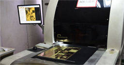
回路が設計と一致し、欠陥がないことを確認するためのデジタル「画像」に対する回路の検査。 ボードのスキャンによって達成され、それから訓練された検査官はスキャンプロセスが強調したどんな異常でも確かめるでしょう。 PCBWayグループは開回路の修理を許可しません。


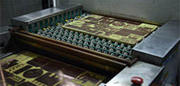
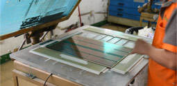
内層には酸化物層が塗布され、次いで層間を絶縁するプリプレグと共に「積み重ね」られ、銅箔が積み重ねの上下に加えられる。 積層工程は、感光性ドライレジストと積層しながら、内層を極端な温度(375°F)および圧力(275から400psi)下に置くことからなる。 PCBを高温で硬化させ、圧力をゆっくり解放し、次いで材料をゆっくり冷却する。


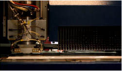
私達は今多層PCBの中で電気接続を後で作成する穴をあけなければならない。 これは、すべての内層接続に対して位置合わせを行うことができるように最適化する必要がある機械的穴あけプロセスです。 この工程でパネルを積み重ねることができる。 穴あけはまたレーザーのドリルによってすることができます

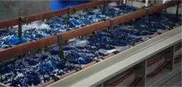
めっきプロセスの最初のステップは、穴の壁に銅の非常に薄い層を化学蒸着することです。
PTHは穴の壁とパネル全体を覆う非常に薄い銅の堆積物を提供します。 信頼性の高い銅の析出物を非金属製の穴の壁にもメッキできるように厳密に制御する必要がある複雑な化学プロセス。 それ自体では十分な量の銅ではないが、我々は今や層間と孔を通して電気的に連続している。パネルめっきはPTH堆積物の上により厚い銅堆積物、典型的には5〜8μmを提供するために続く。 この組み合わせは、トラックおよびギャップの要求を達成するために、メッキおよびエッチングされる銅の量を最適化するために使用されます。


内層プロセス(感光性ドライフィルムを使用した画像転写、UV光への露光、エッチング)と似ていますが、主な違いが1つあります - 銅/定義回路を残したい部分でドライフィルムを削除します。 プロセスの後半で銅。
プロセスのこのステップはクリーンルームで行われます。


追加のめっきがドライフィルム(回路)のない領域に堆積される第二の電解めっき段階。 銅がメッキされると、メッキされた銅を保護するためにスズが塗布されます。


これは通常3段階のプロセスです。 最初のステップは青いドライフィルムを取り除くことです。 2番目のステップは、露出した/不要な銅をエッチング除去する一方で、スズの堆積物が必要な銅を保護するエッチレジストとして機能するようにすることです。 最後の3番目のステップは、回路を離れる錫メッキを化学的に除去することです。


内層AOIの場合と全く同様に、画像形成されエッチングされたパネルは、回路が設計を満たし、それが欠陥がないことを確実にするために走査される。 PCBWayの要求により、開回路の修理はできません。

ソルダーマスクインキはPCB表面全体に塗布されます。 アートワークとUV光を使用して、特定の領域をUVにさらし、露光されていない領域(通常ははんだ付け可能な表面として使用される領域)を除去します。 残りのソルダーマスクはそれから完全に硬化されてそれを弾力のある仕上げにする。 プロセスのこのステップはクリーンルームで行われます。

次いで、露出した銅領域に様々な仕上げが施される。 これは表面の保護と良好なはんだ付け性を可能にするためです。 さまざまな仕上げには、無電解ニッケル液浸金、HASL、液浸銀などがあります。厚さとはんだ付け性のテストは常に行われます。


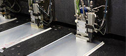
これは、ガーバーデータで定義されている顧客の設計に基づいて、製造パネルを特定のサイズと形状に切断するプロセスです。 配列を提供したりパネルを売ったりするときに利用できる3つの主なオプションがあります - 得点、ルーティングまたはパンチ。 すべての寸法は、パネルの寸法が正しいことを確認するために、お客様から提供された図面に対して測定されます。


トラックとスルーホールの相互接続の完全性をチェックするために使用されます - 完成したボード上に開回路や短絡がないことを確認するためにチェックします。 2つのテスト方法があります。小体積用のフライングプローブと体積用のフィクスチャです。すべてのPCBを元のボードデータと電気的にテストします。 フライングプローブテスターを使用して、各ネットをチェックして、ネットが完全であり(開回路がない)、他のネットと短絡していないことを確認します。


プロセスの最後のステップでは、鋭い目の検査官のチームが各PCBに最終の慎重なチェックオーバーを行います。合格基準に照らしてPCBを視覚的に検査し、PCBWay「承認」検査員を使用します。 手動の目視検査とAVIを使用する - PCBとガーバーを比較し、人間の目より速いチェック速度を持ちますが、それでも人間による検証が必要です。 すべての注文は寸法、はんだ付け性などを含む完全な検査も受けます。


ボードは、PCBWayパッケージング要求(ESDなど)に適合する材料を使用して包装され、要求された輸送モードを使用して出荷される前に箱詰めされます。