Summary: In this article, I will show you how to get a student license and create your first project!
Leave a comment if you start using Altium based on this article, and let me know what you think!
Altium has a huge forum for customer feedback on the product, so if you want anything changed, leave a comment there.
https://forum.live.altium.com/
Student License
Firstly we will need to get a Altium License:
https://www.altium.com/solutions/academic-programs/student-licenses
Student licenses are now free for Altium so I will recommend getting a license even if you are a beginner. So far I have 3 friends that have obtained the license, and the initial feedback is that it's smoother than KiCAD and user friendly. The hard part with Altium is the component library. The included ones are absolutely garbage, so I made my own library that I've posted to Github
Import library
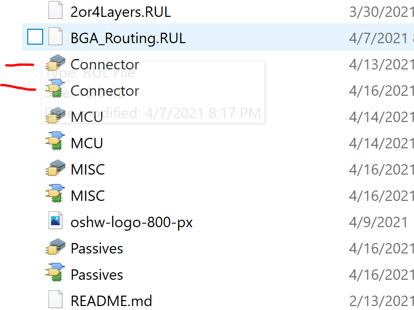
https://github.com/kattemjau/Altium-Lib
Here you will find my component library, I update it with new components regularly. Just clone it or download it as ZIP.
It includes both footprint and schematic symbols. The 3D models are incorporated into the library, but if you are looking for a 3D model, they can usually be found in the 3D model folder.
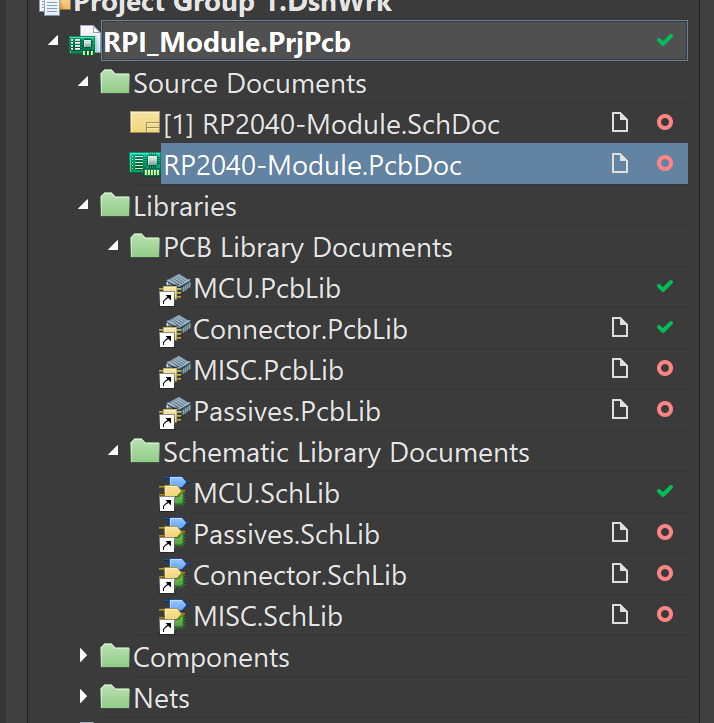
To import a library just double click it or drag it into Altium. These can be compiled and installed into altium, but I usually just add them to projects manually.
Drag them under your project in order to access them in the components view.
Create a new Project
Creating a new project is easy, go to Files->NEW->Project
Add a schematic with right clicking on the project, add new to project and schematic.
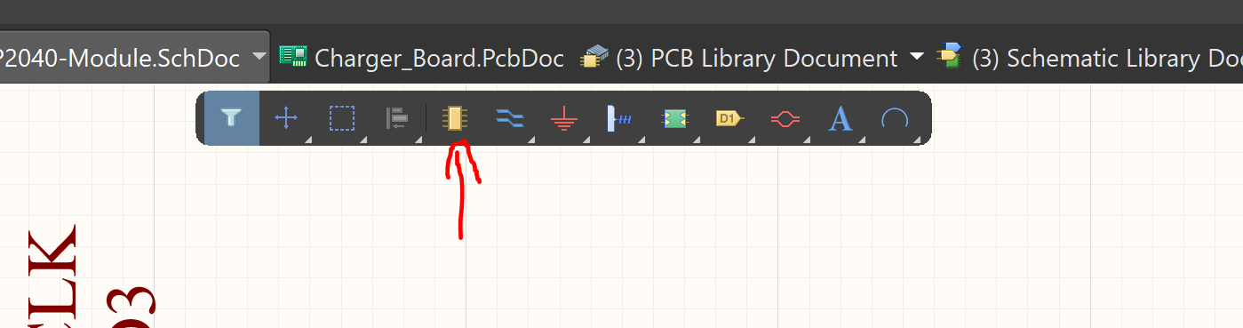
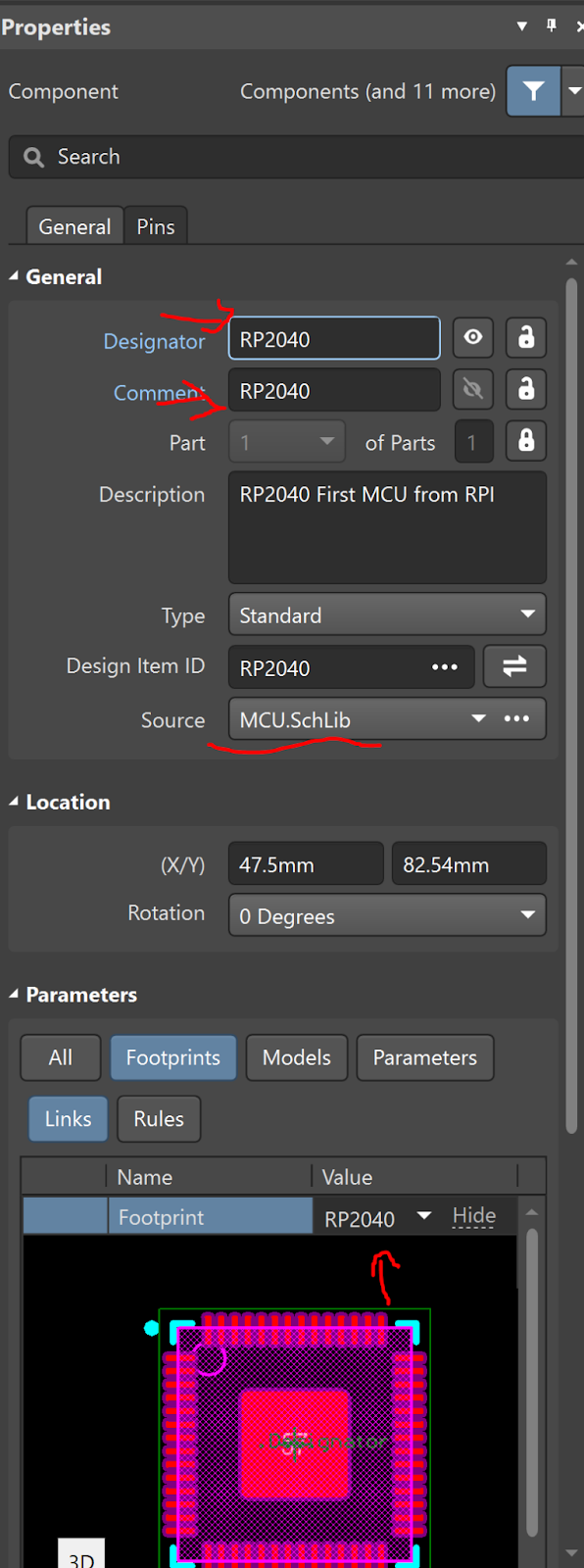
In the schematic click place part in order to get the parts view on the right side.
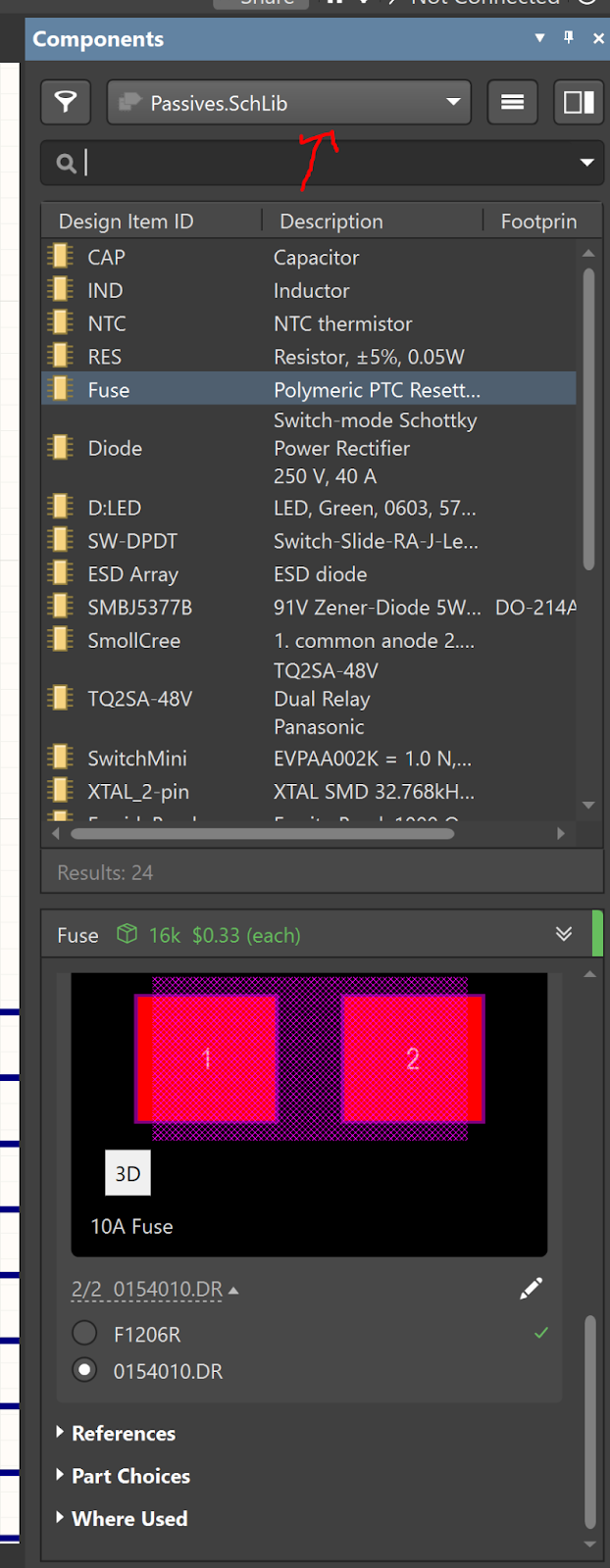
On the right side, this panel will pop up. If you added the library files in the first step, you can now select them here. You can also install the library’s so you no longer need to import them into your projects. Select the component you want to place, and make your schematic. Some components have the same schematic, but different footprints, the footprints can be selected at the bottom here, or later in schematic after selecting the component and going into properties
PROTIP: Double clicking on a component selects it and opens properties
Here you can change the footprint to a different variant
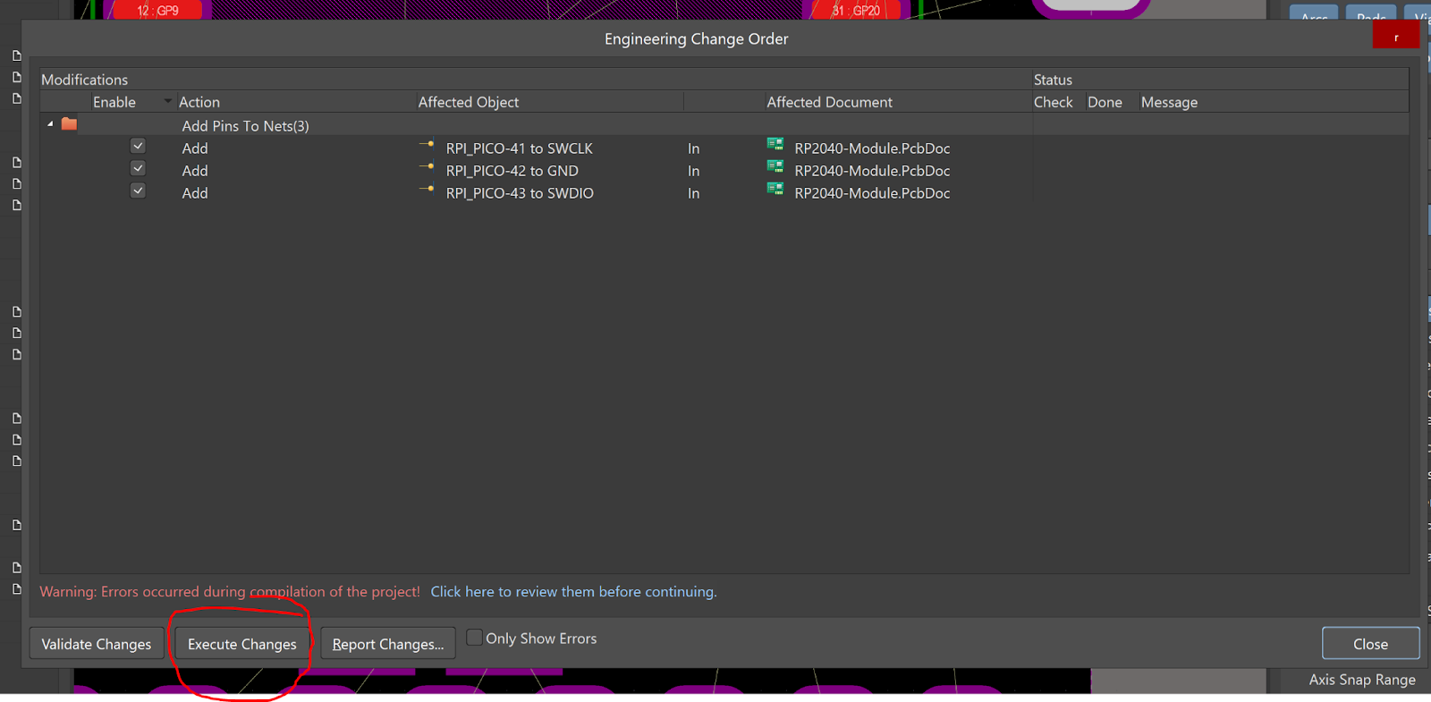
After finishing your schematic, and changing the PCB layout, go to Design->Update PCB
Click Execute changes to export the changes to the Layout. It will give you a message if something is wrong
PROTIP: In layout view, changing between the different views, click 2 for 2D, 3 for 3D and 1 for planning mode.
I will go over the most important things, most things you will easily learn by just using the program.
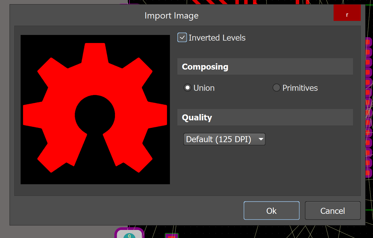
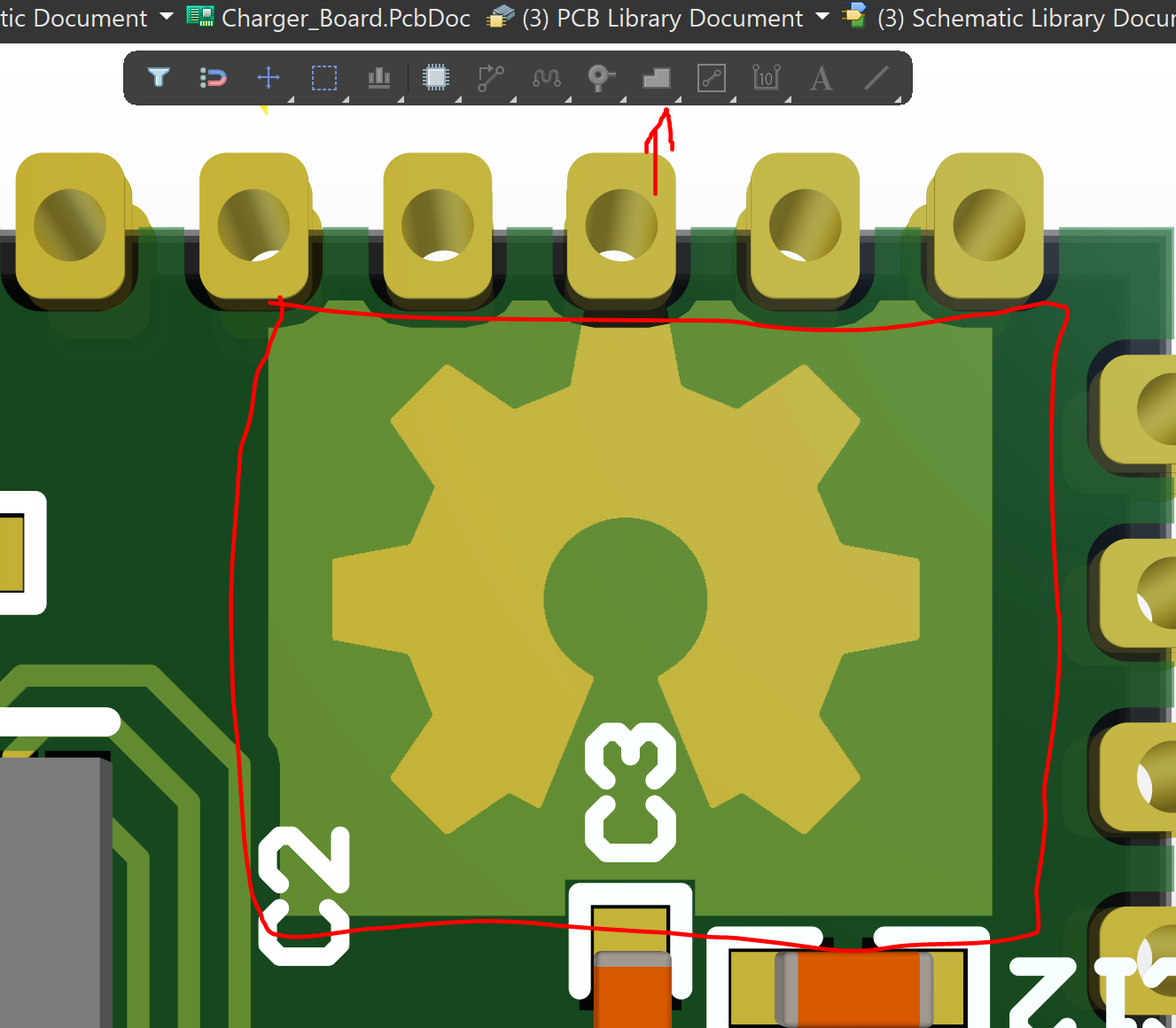
Import an image with Place->Graphics
Select an area where you want it, and select the image that comes in my Altium Lib folder. This is the logo for the Open Hardware Association. It means that your project is open source.
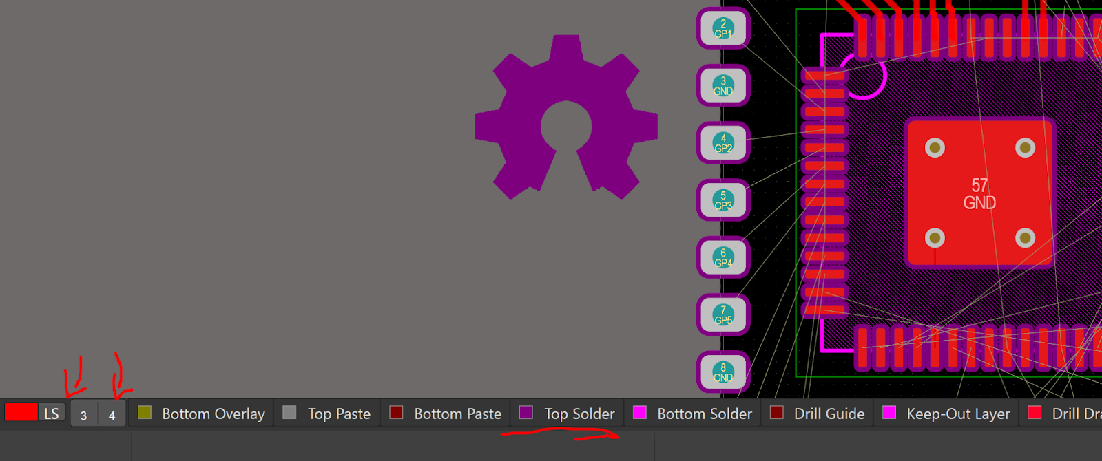
If you want it on the silkscreen layer, select the Top overlay in properties, If you want it to remove the green mask, to expose the copper layer below, choose Top Solder.
The graphic will change color to the layer it's on, and will be visible in 3D mode. In order to show the copper below, you need a polygon with copper pour.
In 2D, click on the new polygon button, holding it in gives you several options. Make your polygon and change what layer you want it on. After reporting the polygon it is now visible in 3D view as a golden Graphic! :)
PROTIP: In 3D, click CTRL+F to rotate the model, 0 to center it, 9 and 8 for different views. Rotating with Shift + Click.
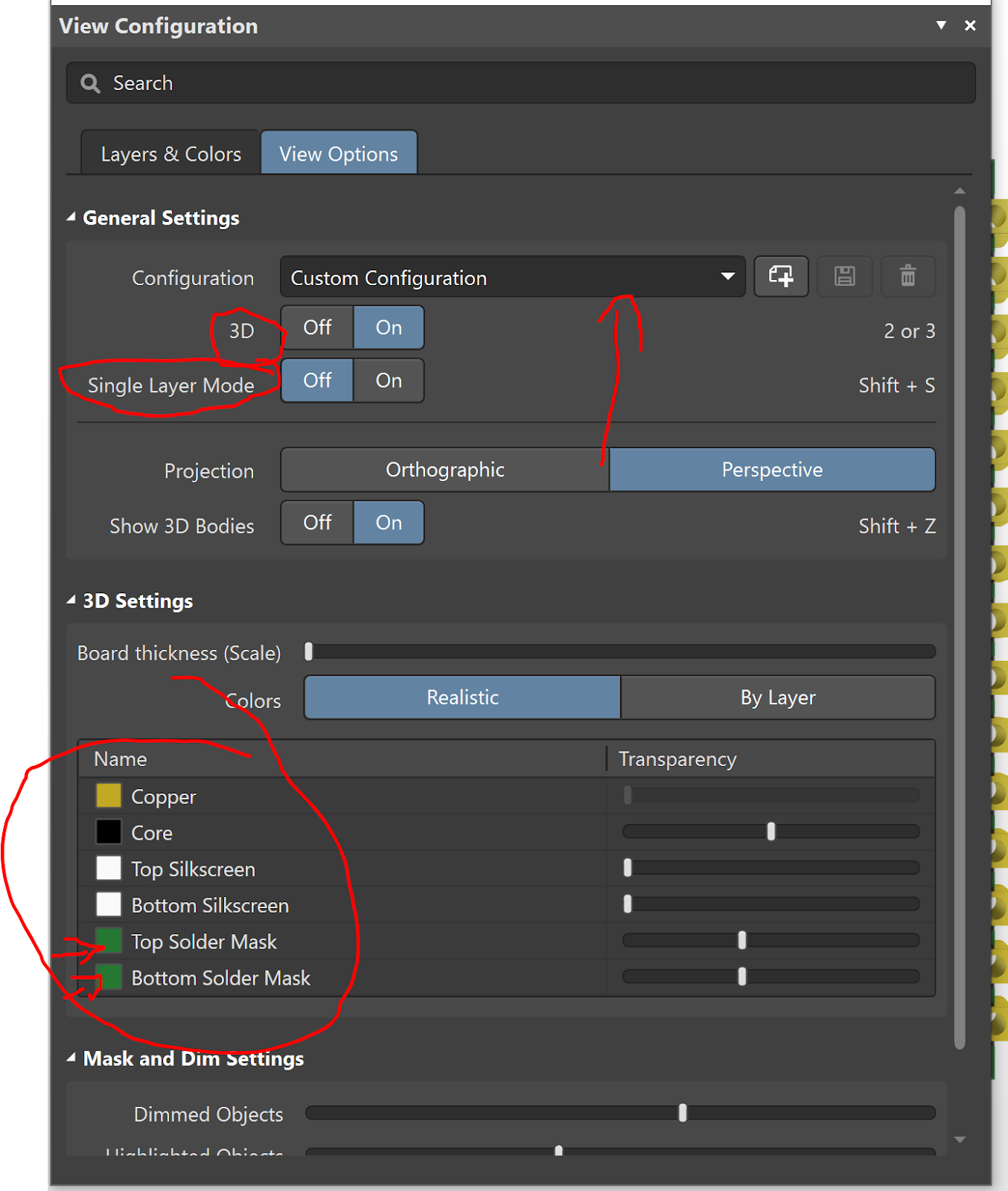
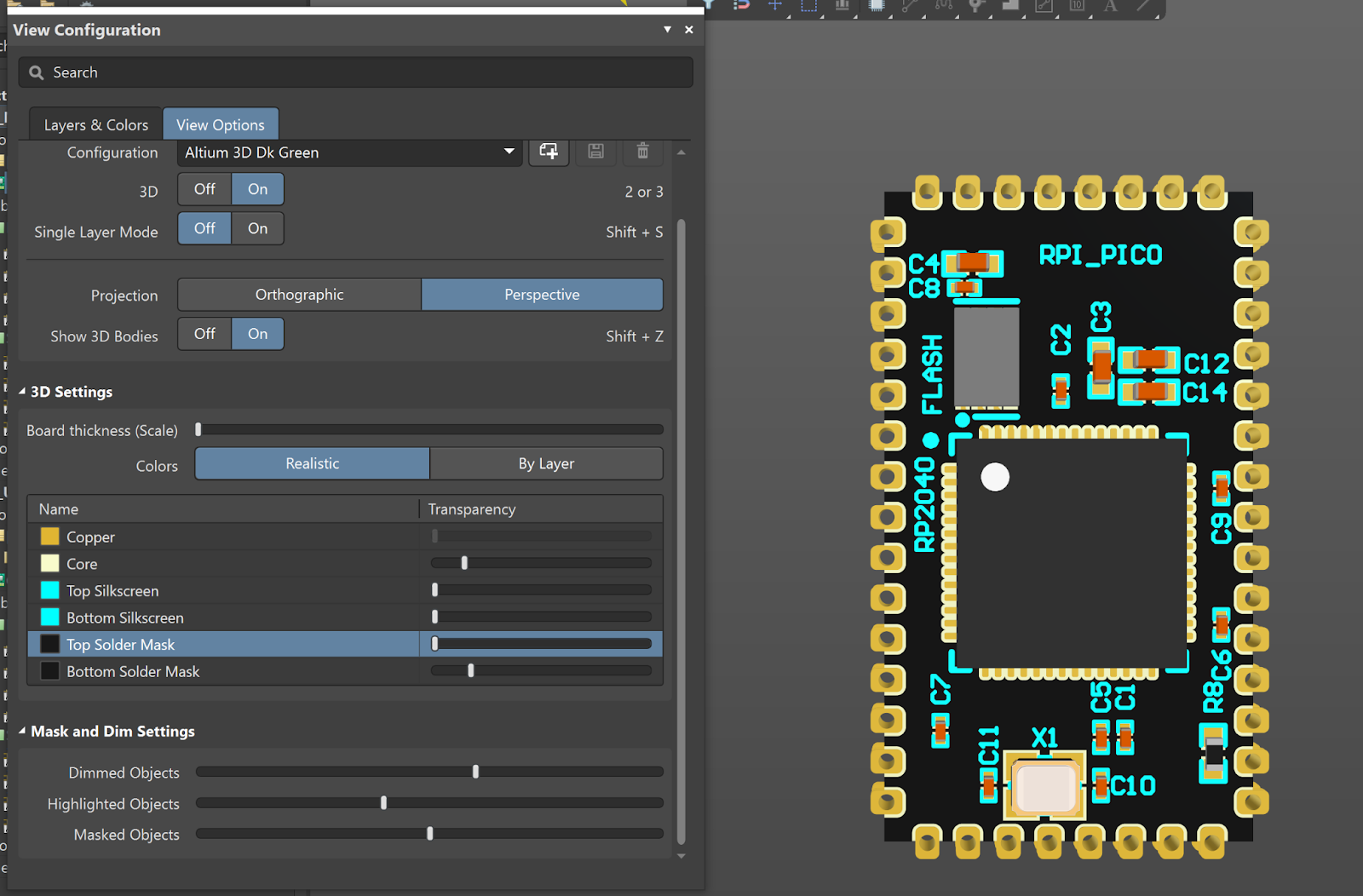
The most important feature, is changing the colour of the PCB:
Go to panels, in the bottom right corner.->View Configuration-> View Options
Here you can switch between different view modes, like a black pcb, purple pcb, 2D transparent is by far my favorite when you are working in cross layers!
Cyan on Matte Black, or Light Green on White are stunning combinations! I'm still looking for a PCB manufacturer that can do dual or tri Overlay colours, might this be something for PCBWay? Transparent Solder mask is also pretty cool, since you can see the traces;)
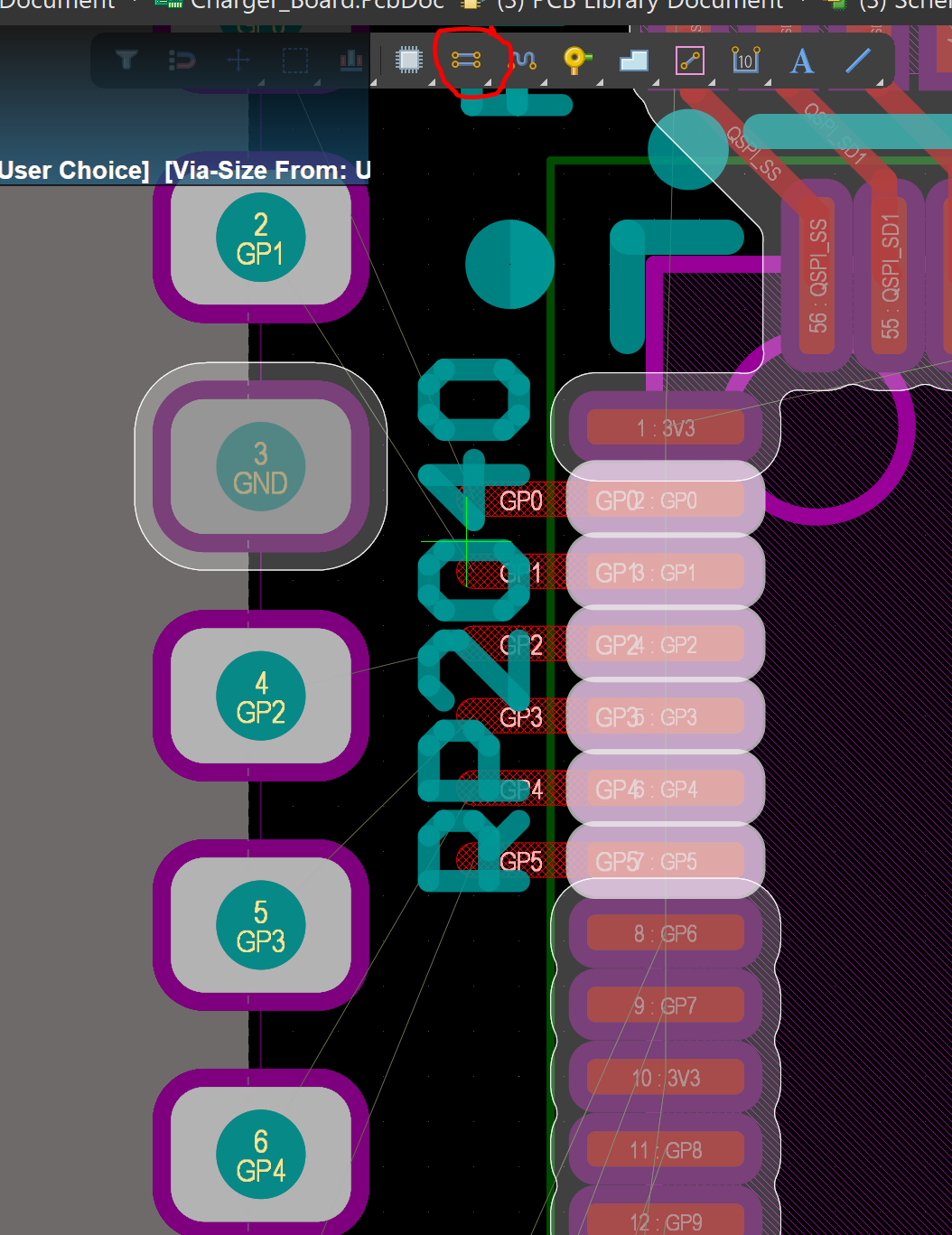
Using the Multi routing, you first need to select the pads, by holding shift + click. Then select the multi route option. If possible to autoroute the last step hit CTRL+ENTER to autoroute the last step. Thewhite areas indicate the distance required to comply with the design rules.
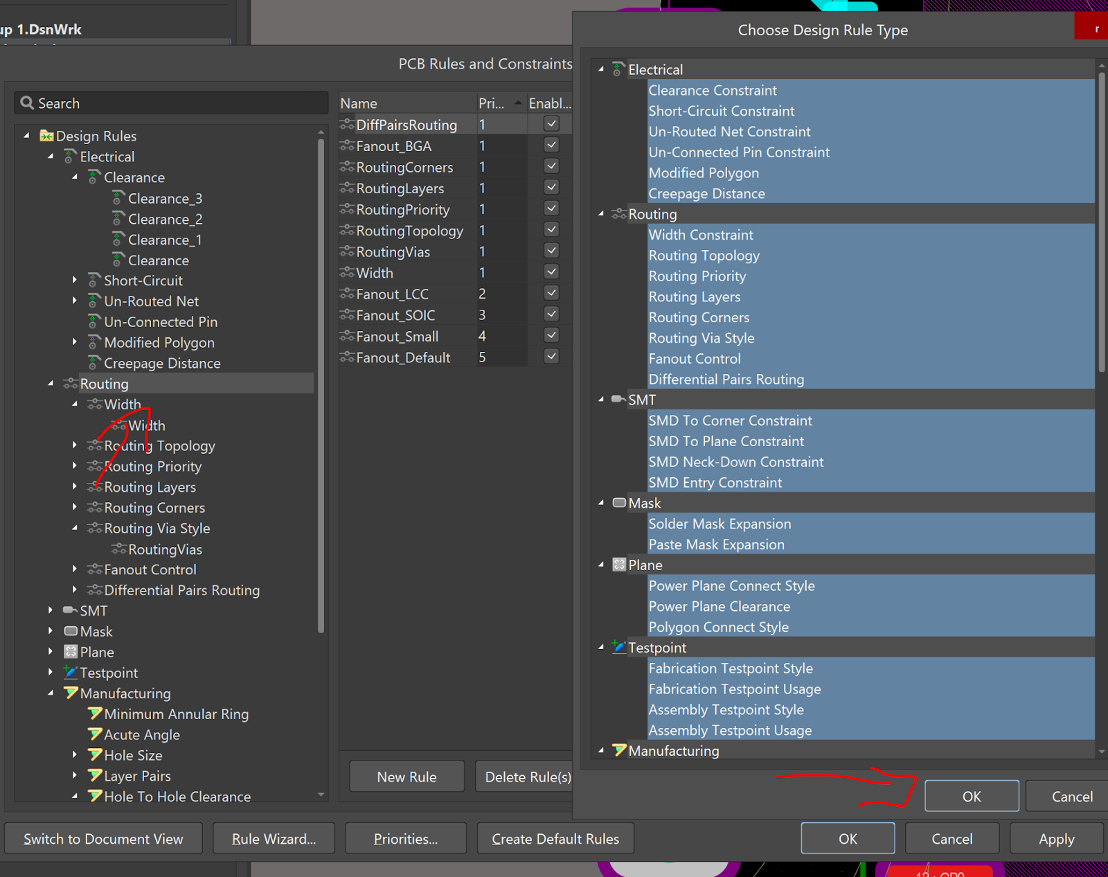
The default design rules are absolute garbage! To change them go do
Design->Rules
Right click on the left, choose import rules.
In the next window select all by CTRL+A, and hit OK
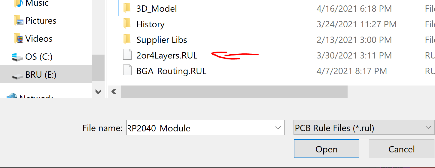
Navigate to the Altium Lib folder you downloaded from Github earlier, and choose the 2 layers rule. This should be compliant with PCBWay Design Capabilities.
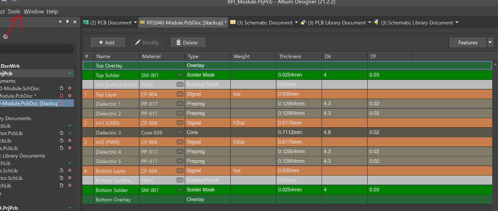
Another thing that is optional, is the layer stack manager, this is important in more advanced multi layer designs. Go to Tools->Presets->2 Layer, and you will get a standard 1.6mm 2 layer pcb. Here you can do impedance tuning and add different via types.
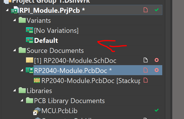
Variants is a really cool feature in Altium. Use it to hide 3D models and remove components from Pick and place files and BOM.
Right click the project, add variant, call it default, click on the component to hide or place it. Hit OK when you are finished
Select your variant here: Note that your export files will also change. You can select the variant to export during the export, usually I forget this :)
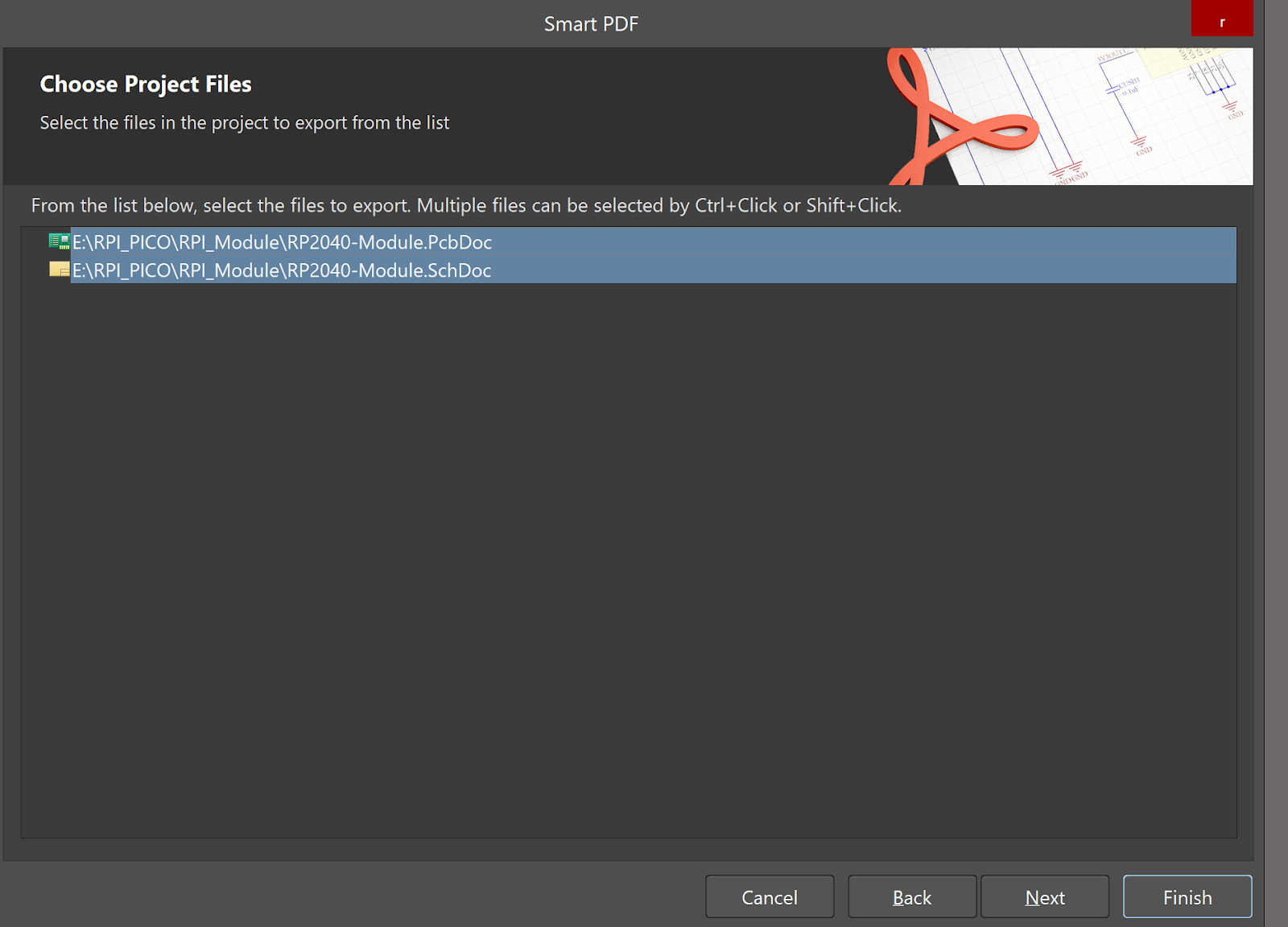
Export your project as a PDF:
File->Smart PDF
Go through the setting, choose what parts to export, do you want to export as a variant? With the BOM? And include the X Ray view of the PCB?
Hit finish to get the PDF
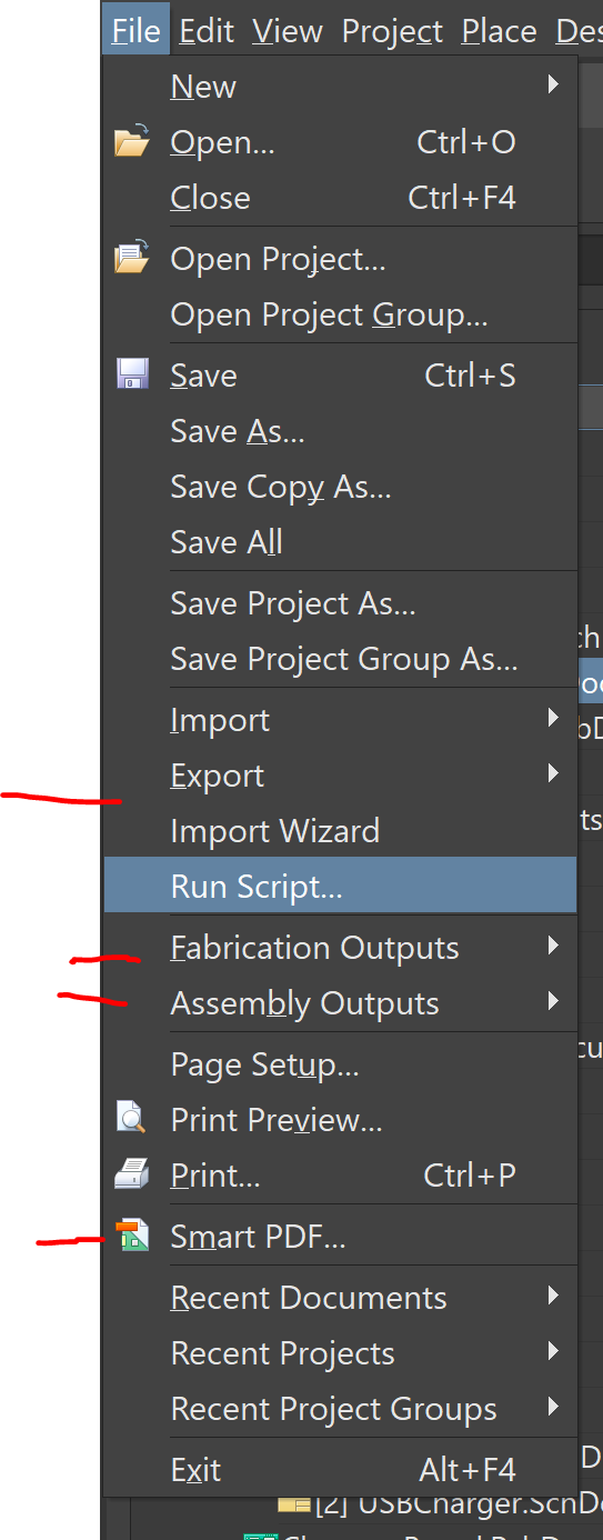
Here you can export a step file of the pcb, the gerber files and pick and place files under assembly outputs.
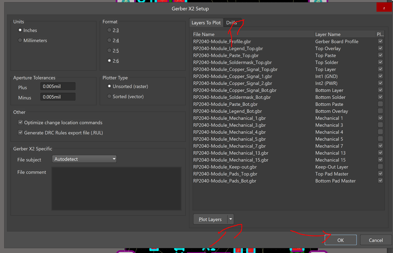
To export GerberX2 under Fabrication Outputs,
Do plot used layers, also under drills hit OK. Then it will export the project and open the gerber viewer.
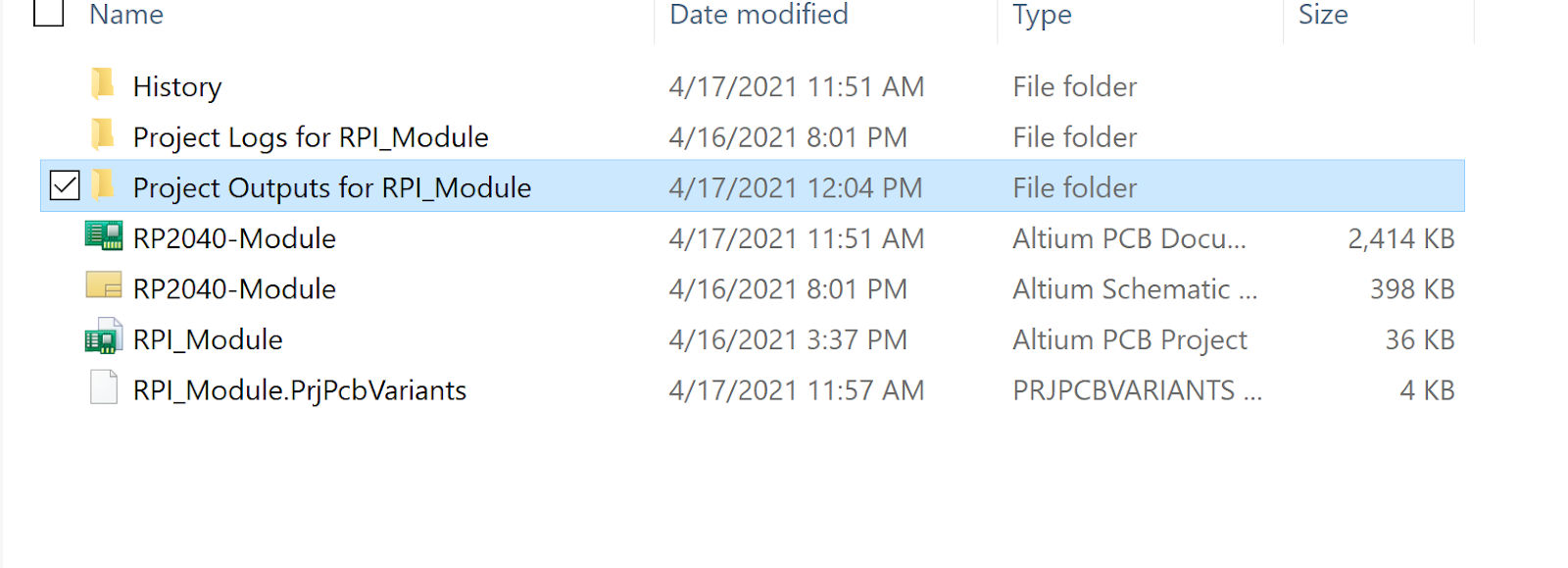
Your output files will be in the project output folder, right click and compress to a zip file before uploading to PCBWay
Now you are ready to make your first project with Altium!
Let me know in the comments what you think about Altium, and make some cool projects.
If you have any questions Join the Voidstar Discord coven: https://discord.gg/voidstarlab